 Deutsch
 English
 Español
 Français
 Italiano
 Nederlands
 Polski
 Português
 Русский
 Türkçe
 Svenska
 Chinese
 Magyar
Intel Core 2 Duo T8300 vs Intel Core i5-520UM vs Intel Core 2 Duo T9900
Intel Core 2 Duo T8300
► remove from comparisonThe Intel Core 2 Duo T8300 was at the time of announcement a fast dual-core CPU for laptops with 3 MB level 2 cache. It is based on the Penryn core with all features enabled (but without the full 6MB level 2 cache). The later announced Core 2 Duo P7450 was cheaper and used less power.
Intel Core i5-520UM
► remove from comparison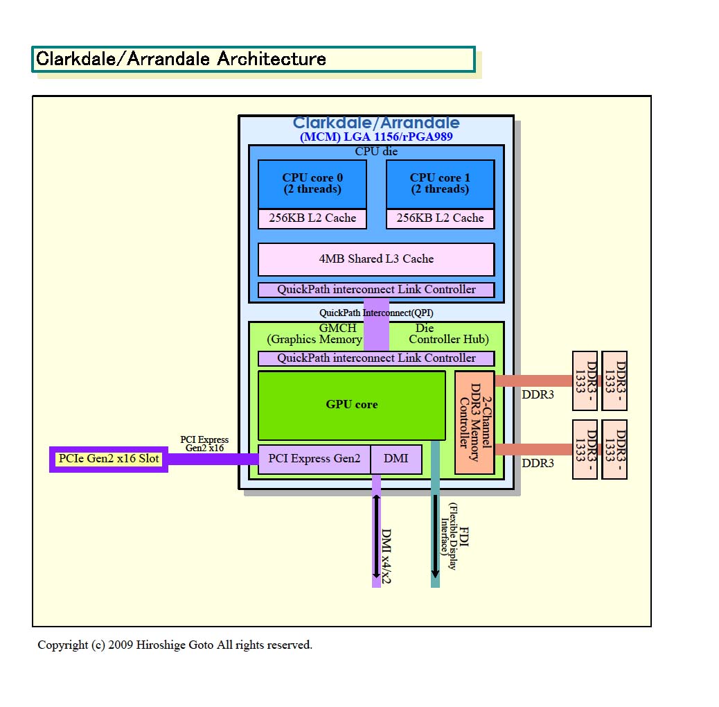
The Intel Core i5-520UM is a Ultra Low Voltage dual-core processor for small and light laptops. It is clocked with 1.06 - 1.86 GHz (if Turbo Boost is enabled). Each core is based on the Nehalem (Westmere) micro-architecture. Hyperthreading enables the Dual Core CPU to handle 4 threads at once (for a better usage of the pipeline). Compared to the Core i7-620UM, the i5 offers only 3MB Level 3 cache (i7 4MB) and a lower maximum Turbo Boost frequency. Other Core i5 CPUs (withouth the U in the name) are faster due to the higher clock speed, but need more power.
A feature of the new Core i5-520UM is the integrated graphics card (called Intel HD Graphics) and memory controller. Both are on a separate die that is still manufactured in 45nm whereas the CPU die is already manufactured in the new 32nm process.
Due to the integrated memory controller, the HyperThreading and Turbo Boost, the Core i5-520UM is faster than a similar clocked Core 2 Duo (1.2 GHz) in all (us known) applications and benchmarks. Still the Turbo Boost may not trigger very often (sometimes it is even not activated in the BIOS) and therefore the maximum of 1.86 GHz is not very important.
The 32nm cpu cores of the Westmere generation can also process some new instructions to accelerate AES encryptions. Modern applications that support AES encoding can profit significantly using the new instructions (e.g. the Communications Suite test in the PCMark Vantage boosts up to 70% using AES in the faster Core i5-520M).
The integrated Intel Graphics Media Accelerator HD (GMA HD) graphics card is between 166-500 MHz (Turbo Boost) and therefore the base speed is clearly below the non low voltage versions. The performance should still be faster than the old GMA 4500MHD.
The power consumption of 18 Watt TDP (max.) counts for the whole package and therefore it is clearly better than the 17 Watt TDP of the Core 2 Duo SL-series (CPU alone).
Intel Core 2 Duo T9900
► remove from comparison
The Intel Core 2 Duo T9900 is the theoretical successor of the Core 2 Extreme X9100 (which also clocks at 3.06 GHz) that uses less power due to the modern stepping and the Enhanced Halt State (C1E). The only advantage of the X9100 is the free multiplikator (which allows easy overclocking of the CPU).
The T9900 is a fast dual core CPU for laptops which features 6 MB of shared level 2 cache and a TDP of 35 Watt. Due to the high clock speed, modern games (in 2009) should not be limited by the CPU speed. For single threaded applications it is one of the fastest CPUs for laptops (only beaten by the new Core i7 with enabled Turbo mode).
The T9900 uses a Penryn (Montevina Update) core that features 2 integer units, 1 floating point unit, 1 load unit, and 1 store unit in a 14-stages long pipeline. Due to the Wide Dynamic Execution Technology, the core is able to simultaneously execute up to four instructions.
The integrated Enhanced Speedstep is able to downclock the core dynamically as low as 800 MHz to save power (in idle mode).
The Core 2 Duo T9900 can be used in a Socket P socket with 479 pins: Socket P / Micro Flip-Chip Pin Grid Array (Micro-FCPGA) requires 479-pin surface mount Zero Insertion Force (ZIF) socket (mPGA479M socket) or Micro Flip-Chip Ball Grid Array (Micro-FCBGA) for surface mount (479-ball).
| Model | Intel Core 2 Duo T8300 | Intel Core i5-520UM | Intel Core 2 Duo T9900 | ||||||||||||||||||||||||||||||||||||||||||||||||||||
| Series | Intel Core 2 Duo | Intel Core i5 | Intel Core 2 Duo | ||||||||||||||||||||||||||||||||||||||||||||||||||||
| Codename | Penryn | Arrandale | Penryn | ||||||||||||||||||||||||||||||||||||||||||||||||||||
| Series: Core 2 Duo Penryn |
| ||||||||||||||||||||||||||||||||||||||||||||||||||||||
| Clock | 2400 MHz | 1060 - 1866 MHz | 3060 MHz | ||||||||||||||||||||||||||||||||||||||||||||||||||||
| FSB | 800 | 2500 | 1066 | ||||||||||||||||||||||||||||||||||||||||||||||||||||
| L2 Cache | 3 MB | 512 KB | 6 MB | ||||||||||||||||||||||||||||||||||||||||||||||||||||
| Cores / Threads | 2 / 2 | 2 / 4 | 2 / 2 | ||||||||||||||||||||||||||||||||||||||||||||||||||||
| TDP | 35 Watt | 18 Watt | 35 Watt | ||||||||||||||||||||||||||||||||||||||||||||||||||||
| Transistors | 410 Million | 382+177 Million | 410 Million | ||||||||||||||||||||||||||||||||||||||||||||||||||||
| 45 nm, 1-1.25V | 32 nm | 45 nm, 1.05-1.2125 V | |||||||||||||||||||||||||||||||||||||||||||||||||||||
| Die Size | 107 mm2 | 81+114 mm2 | 107 mm2 | ||||||||||||||||||||||||||||||||||||||||||||||||||||
| max. Temp. | 105 °C | 105 °C | 105 °C | ||||||||||||||||||||||||||||||||||||||||||||||||||||
| Socket | BGA479, PGA478 | BGA1288 | Socket P (BGA479, PGA478) | ||||||||||||||||||||||||||||||||||||||||||||||||||||
| Features | Virtualization (VT-x), Intel 64, Idle States, Enhanced Speedstep, Execute Disable Bit | Turbo Boost (1.86 GHz max), Hyper Threading, Enhanced Speedstep, integrated GMA HD 166-500MHz | SSE4.1, Virtualization Technology, Execute Disable Bit, Enhanced Speedstep, Ehnaced Halt State (C1E), 64 Bit, Trusted Execution Technology | ||||||||||||||||||||||||||||||||||||||||||||||||||||
| Architecture | x86 | x86 | x86 | ||||||||||||||||||||||||||||||||||||||||||||||||||||
| $241 U.S. | $241 U.S. | $530 U.S. | |||||||||||||||||||||||||||||||||||||||||||||||||||||
| Announced | |||||||||||||||||||||||||||||||||||||||||||||||||||||||
| Manufacturer | ark.intel.com | ark.intel.com | ark.intel.com | ||||||||||||||||||||||||||||||||||||||||||||||||||||
| L3 Cache | 3 MB | ||||||||||||||||||||||||||||||||||||||||||||||||||||||
| L1 Cache | 128 KB |

