 Deutsch
 English
 Español
 Français
 Italiano
 Nederlands
 Polski
 Português
 Русский
 Türkçe
 Svenska
 Chinese
 Magyar
AMD Ryzen 5 4680U vs Intel Core i5-1034G1
AMD Ryzen 5 4680U
► remove from comparison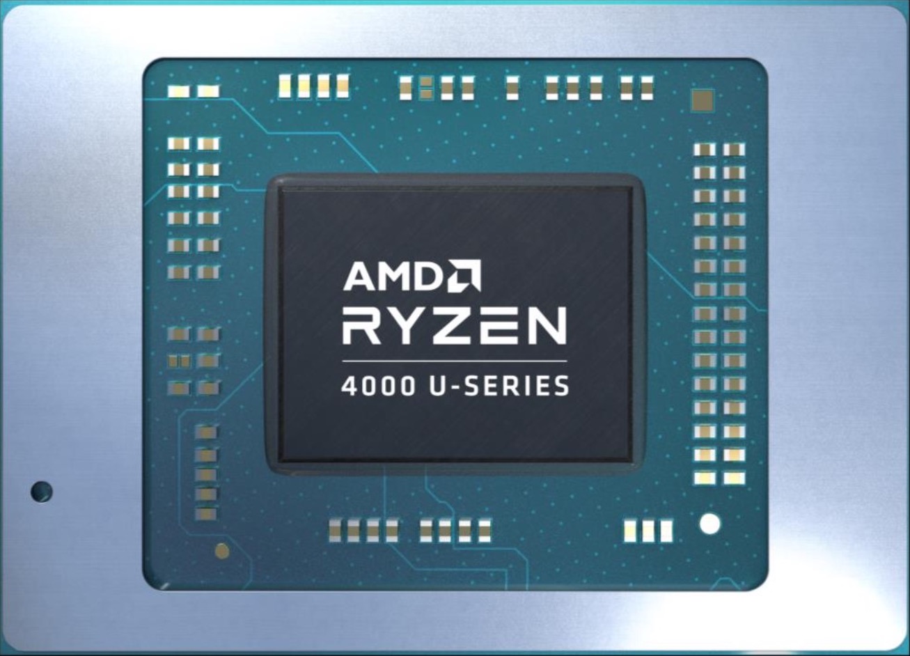
The AMD Ryzen 5 4680U is a semi-custom APU of the Renoir family designed for Microsoft devices. The 4680U integrates six CPU cores based on the Zen 2 microarchitecture clocked at 2.2 GHz (base) to 4 GHz (Boost) with SMT support for a total 12 threads. The two advantages a 4680U has over the older Ryzen 5 4600U are its higher base clock speed and a faster iGPU.
Architecture
The chip is manufactured on the modern 7 nm TSMC process and in part thanks to this fact, AMD advertises a 2x performance per watt improvement over the 12 nm Ryzen 3000 mobile processors. The built-in dual-channel memory controller supports LPDDR4-4266 RAM. Furthermore, 8 MB of L3 cache can be found on the chip.
Just like the other mobile Ryzen 4000 CPUs, a 4680U supports PCI-Express 3.0. Please go to our Renoir processor hub page for additional information on the product family.
Performance
Multi-thread performance is most comparable to the Ryzen 7 4700U and the Core i5-10500H, the latter being a much more power-hungry chip. This makes the Ryzen a more than decent CPU for most tasks, as of early 2022.
Graphics
In addition to the six CPU cores, the APU also integrates a DX 12 compatible Radeon RX Vega 7 graphics adapter with 7 CUs (448 unified shaders) at up to 1,500 MHz. The Vega iGPU will have no trouble HW-decoding AVC, HEVC and VP9 videos, but the newer AV1 codec will only be decoded via software. In terms of gaming, we are looking at an MX150-level performance. Pretty much all games released in 2020 can be played on low to medium settings in 720p on this graphics adapter.
Power consumption
This Ryzen 5 series chip has a default TDP (also known as the long-term power limit) of 15 W, a value that laptop makers - Microsoft, in this case - are free to change to anything between 10 W and 25 W, with clock speeds and performance changing accordingly as a result. Indeed, we saw the CPU consume roughly 23 watts when subjected to our usual stress testing routine.
The 7 nm TSMC process this Ryzen is built with makes for very decent, as of mid 2022, energy efficiency.
Intel Core i5-1034G1
► remove from comparisonThe Intel Core i5-1034G1 is a power efficient quad-core SoC for laptops and Ultrabooks based on the Ice -Lake-U generation that was announced in Mai 2019 (Computex). It integrates four Sunnycove processor cores (8 threads thanks to HyperThreading) clocked at 0.8 (base) - 3.6 (single core Turbo) GHz. 2 cores can reach 3.6 GHz and all four 3.3 GHz using Turbo Boost. According to Intel the Sunnycove cores achieve 18% more IPCs (Instructions per Clock) and therefore the CPU performance should be similar to the higher clocked Whiskey-Lake predecessors (e.g. Core i5-8365U with up to 4.1 GHz).
The biggest improvement for Ice-Lake is the integrated Gen 11 graphics card called UHD Graphics G1. The Core i5-1034G1 integrates the smallest GPU, the UHD Graphics that features 32 of the 64 CUs and clocks at 300 - 1050? MHz. The faster variants include Iris Plus G4 and G7.
Other improvements for Ice Lake are the AI hardware acceleration and the partial integration of Thunderbolt and Wifi 6 in the chip. The integrated DDR4 memory controller supports modules with up to 3200 MHz (and LPDDDR4 3733).
The Core i5-1034G1 is produced in the improved 10nm+ process at Intel (2nd generation) that should offer a comparable performance to the 7nm process at TSMC. The TDP is specified at 15 Watts and therefore the CPU can be used in thin and light laptops (but usually with a fan). Intel offers a configurable TDP of 7.5 - 25 Watts for the partners resulting in significant performance differences (due to longer periods of Turbo Boost).
| Model | AMD Ryzen 5 4680U | Intel Core i5-1034G1 | ||||||||||||||||||||||||||||||||||||
| Series | AMD Renoir (Ryzen 4000 APU) | Intel Ice Lake | ||||||||||||||||||||||||||||||||||||
| Codename | Renoir-U (Zen 2) | Ice Lake U | ||||||||||||||||||||||||||||||||||||
| Series: Ice Lake Ice Lake U |
|
| ||||||||||||||||||||||||||||||||||||
| Clock | 2200 - 4000 MHz | 800 - 3600 MHz | ||||||||||||||||||||||||||||||||||||
| L1 Cache | 384 KB | 192 KB | ||||||||||||||||||||||||||||||||||||
| L2 Cache | 3 MB | 2 MB | ||||||||||||||||||||||||||||||||||||
| L3 Cache | 8 MB | 6 MB | ||||||||||||||||||||||||||||||||||||
| Cores / Threads | 6 / 12 | 4 / 8 | ||||||||||||||||||||||||||||||||||||
| TDP | 15 Watt | 15 Watt | ||||||||||||||||||||||||||||||||||||
| Technology | 7 nm | 10 nm | ||||||||||||||||||||||||||||||||||||
| max. Temp. | 105 °C | |||||||||||||||||||||||||||||||||||||
| Socket | FP6 | |||||||||||||||||||||||||||||||||||||
| Features | LPDDR4-4266 RAM, PCIe 3, MMX, SSE, SSE2, SSE3, SSSE3, SSE4A, SSE4.1, SSE4.2, AVX, AVX2, BMI2, ABM, FMA, ADX, SMEP, SMAP, SMT, CPB, AES-NI, RDRAND, RDSEED, SHA | AVX512, DL Boost, Turbo Boost 2.0 | ||||||||||||||||||||||||||||||||||||
| iGPU | AMD Radeon RX Vega 7 ( - 1500 MHz) | Intel UHD Graphics G1 (Ice Lake 32 EU) (300 MHz) | ||||||||||||||||||||||||||||||||||||
| Architecture | x86 | x86 | ||||||||||||||||||||||||||||||||||||
| Announced | ||||||||||||||||||||||||||||||||||||||
| Manufacturer | www.amd.com |

