

Intel Processor N100 vs Intel Core i3-1215U vs Intel Celeron 7300
Intel Processor N100
► remove from comparison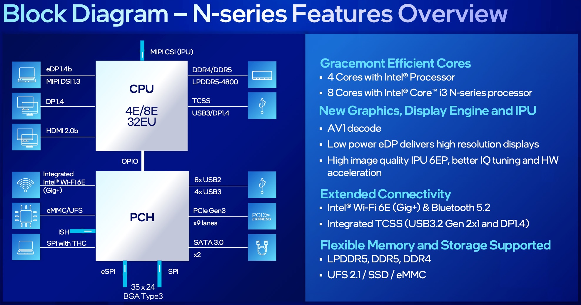
The Intel Processor N100 is an entry-level mobile CPU for thin and light laptops from the Alder Lake-N series. It was announced in early 2023 and offers no performance cores and 4 of the 8 efficient cores (E-cores, Gracemont architecture). The chip does not support HyperThreading and clocks with 1 to 3.4 GHz. The performance of the E-cores should be similar to old Skylake cores (compare to the Core i7-6700HQ). All cores can use up to 6 MB L3-cache.
Performance
The average N100 in our database delivers unimpressive multi-thread benchmark scores that are most similar to those of the Core i3-1115G4. The chip is fast enough for many day-to-day tasks, but not much more than that; the other thing to keep in mind is that of the two N100-toting systems tested by us as of October 2023, both have rather high CPU power limits. The chip will be noticeably slower if limited to just six or seven Watts.
Features
The Alder Lake-N chips only support single channel memory with up to DDR5-4800, DDR4-3200 or LPDDR5-4800. The chip also supports Quick Sync and AV1 decoding (most likely same engine as in Alder Lake). Furthermore, Wi-Fi 6E and Bluetooth 5.2 are partly integrated (but no Thunderbolt). External chips can be connected via PCIe Gen3 x9 (via the PCH).
The integrated graphics adapter is based on the Xe-architecture and offers only 24 of the 32 EUs (Execution Units) operating at only 450 - 750 MHz. Due to the single channel memory, low clock speeds, and low shader count, the gaming performance of the iGPU is very limited.
Power consumption
The N100 has a base power consumption of only 6 W and is therefore suited for fanless cooling. The CPU is built with a further improved 10nm SuperFin process at Intel (called Intel 7).
Intel Core i3-1215U
► remove from comparisonThe Intel Core i3-1215U is a mid-range mobile CPU for thin and light laptops based on the Alder Lake architecture. It was announced in early 2022 and offers 2 performance cores (P-cores, Golden Cove architecture) and 4 efficient cores (E-cores, Gracemont architecture). The P-cores support Hyper-Threading leading to 8 supported threads when combined with the E-cores. The clock rate ranges from 1.2 to 4.4 GHz on the performance cluster and 0.9 to 3.3 GHz on the efficient cluster. The performance of the E-cores should be similar to old Skylake cores (compare to the Core i7-6700HQ). All cores can use up to 10 MB L3-cache. Compared to the faster i5 and i7 models, the i3 does not include vPro features.
Performance
The average 1215U in our database is in the same league as the Ryzen 3 5300U and also the Core i7-1185G7, as far as multi-thread benchmark scores are concerned. This is decent enough of a result, as of late 2022. For an entry-level CPU, that is.
Your mileage may vary depending on how competent the cooling solution of your laptop is, and how high the CPU power limits are.
Features
The integrated memory controller supports various memory types up to DDR5-4800, DDR4-3200, LPDDR5-5200, and LPDDR4x-4267. The Thread Director (in hardware) can support the operating system to decide which thread to use on the performance or efficient cores for the best performance. For AI tasks, the CPU also integrates GNA 3.0 and DL Boost (via AVX2). Quick Sync in version 8 is the same as in the Rocket Lake CPUs and supports MPEG-2, AVC, VC-1 decode, JPEG, VP8 decode, VP9, HEVC, and AV1 decode in hardware. The CPU only supports PCIe 4.0 (x8 for a GPU and two x4 for SSDs).
The integrated graphics card is based on the Xe-architecture and offers 64 of the 96 EUs (Execution Units) operating at up to 1.1 GHz.
The CPU is rated at 15 W base power (TDP, PL1) and 55 W max. Turbo power (PL2) and the whole SoC is manufactured in a 10nm process at Intel, which is known as Intel 7.
Intel Celeron 7300
► remove from comparisonThe Intel Celeron 7300 is an entry-level mobile CPU for thin and light laptops based on the Alder Lake architecture. It was announced in early 2022 and offers one performance core (P-cores, Golden Cove architecture) and 4 efficient cores (E-cores, Gracemont architecture). The CPU does not support HyperThreading leading to only 5 supported threads at once. The clock rate of the performance cluster is 1000 MHz, the one of the efficient cluster is 700 MHz. The performance of the E-cores should be similar to old Skylake cores (compare to the Core i7-6700HQ). All cores can use up to 8 MB L3-cache. Compared to the faster Core i3-1215U, the Celeron offers one less P-core and lower clock speeds (no Turbo).
Performance
Thanks to the 5 cores, the multi-threaded performance should be clearly faster than the older dual-core Tiger Lake CPUs with 15 Watt (like the Intel Core i3-1115G4). However, due to the missing Turbo and the low clock speed, the single core performance will be very low.
Features
The integrated memory controller supports various memory types up to DDR5-4800, DDR4-3200, LPDDR5-5200, and LPDDR4x-4267. The Thread Director (in hardware) can support the operating system to decide which thread to use on the performance or efficient cores for the best performance. For AI tasks, the CPU also integrates GNA 3.0 and DL Boost (via AVX2). Quick Sync in version 8 is the same as in the Rocket Lake CPUs and supports MPEG-2, AVC, VC-1 decode, JPEG, VP8 decode, VP9, HEVC, and AV1 decode in hardware. The CPU only supports PCIe 4.0 (14 lanes combined with Gen 3).
The integrated graphics card is based on the Xe-architecture and offers 48 of the 96 EUs (Execution Units) operating at up to 0.8 GHz.
The CPU is rated at 15 W base power (TDP, PL1) and 55 W max. power (PL2). The minimum assured power is 12 Watt. The whole SoC is manufactured in a 10nm process at Intel, which is known as Intel 7.
| Model | Intel Processor N100 | Intel Core i3-1215U | Intel Celeron 7300 | ||||||||||||||||||||||||||||||||||||||||||||||||||||||||||||||||||||||||||||||||||||||||||||||||||||||||||||||||||||||||||||||||||||||||||||
| Codename | Alder Lake-N | Alder Lake-U | Alder Lake-U | ||||||||||||||||||||||||||||||||||||||||||||||||||||||||||||||||||||||||||||||||||||||||||||||||||||||||||||||||||||||||||||||||||||||||||||
| Series | Intel Alder Lake-N | Intel Alder Lake-M | Intel Alder Lake-M | ||||||||||||||||||||||||||||||||||||||||||||||||||||||||||||||||||||||||||||||||||||||||||||||||||||||||||||||||||||||||||||||||||||||||||||
| Series: Alder Lake-M Alder Lake-U |
|
|
| ||||||||||||||||||||||||||||||||||||||||||||||||||||||||||||||||||||||||||||||||||||||||||||||||||||||||||||||||||||||||||||||||||||||||||||
| Clock | 1000 - 3400 MHz | 900 - 4400 MHz | 700 - 1000 MHz | ||||||||||||||||||||||||||||||||||||||||||||||||||||||||||||||||||||||||||||||||||||||||||||||||||||||||||||||||||||||||||||||||||||||||||||
| L3 Cache | 6 MB | 10 MB | 8 MB | ||||||||||||||||||||||||||||||||||||||||||||||||||||||||||||||||||||||||||||||||||||||||||||||||||||||||||||||||||||||||||||||||||||||||||||
| Cores / Threads | 4 / 4 4 x 3.4 GHz Intel Crestmont E-Core | 6 / 8 | 5 / 5 1 x 1.0 GHz Intel Golden Cove P-Core 4 x 0.7 GHz Intel Crestmont E-Core | ||||||||||||||||||||||||||||||||||||||||||||||||||||||||||||||||||||||||||||||||||||||||||||||||||||||||||||||||||||||||||||||||||||||||||||
| TDP | 6 Watt | 15 Watt | 9 Watt | ||||||||||||||||||||||||||||||||||||||||||||||||||||||||||||||||||||||||||||||||||||||||||||||||||||||||||||||||||||||||||||||||||||||||||||
| Technology | 10 nm | 10 nm | 10 nm | ||||||||||||||||||||||||||||||||||||||||||||||||||||||||||||||||||||||||||||||||||||||||||||||||||||||||||||||||||||||||||||||||||||||||||||
| max. Temp. | 105 °C | 100 °C | 100 °C | ||||||||||||||||||||||||||||||||||||||||||||||||||||||||||||||||||||||||||||||||||||||||||||||||||||||||||||||||||||||||||||||||||||||||||||
| Socket | BGA1264 | BGA1744 | BGA1700 | ||||||||||||||||||||||||||||||||||||||||||||||||||||||||||||||||||||||||||||||||||||||||||||||||||||||||||||||||||||||||||||||||||||||||||||
| Features | DDR4-3200/DDR5-4800/LPDDR5-4800 RAM (sin. chan.), PCIe 3, GNA, MMX, SSE, SSE2, SSE3, SSSE3, SSE4.1, SSE4.2, AVX, AVX2, BMI2, ABM, FMA, ADX, VMX, SMEP, SMAP, EIST, TM1, TM2, Turbo, SST, AES-NI, RDRAND, RDSEED, SHA | DDR4-3200/LPDDR4x-4266/DDR5-4800/LPDDR5-5200 RAM, PCIe 4, Thr. Dir., DL Boost, GNA, MMX, SSE, SSE2, SSE3, SSSE3, SSE4.1, SSE4.2, AVX, AVX2, BMI2, ABM, FMA, ADX, SMEP, SMAP, EIST, TM1, TM2, HT, Turbo, SST, AES-NI, RDRAND, RDSEED, SHA | Thread Director | ||||||||||||||||||||||||||||||||||||||||||||||||||||||||||||||||||||||||||||||||||||||||||||||||||||||||||||||||||||||||||||||||||||||||||||
| iGPU | Intel UHD Graphics 24EUs (Alder Lake-N) ( - 750 MHz) | Intel UHD Graphics 64EUs (Alder Lake 12th Gen) ( - 1100 MHz) | Intel UHD Graphics Xe G4 48EUs ( - 800 MHz) | ||||||||||||||||||||||||||||||||||||||||||||||||||||||||||||||||||||||||||||||||||||||||||||||||||||||||||||||||||||||||||||||||||||||||||||
| Architecture | x86 | x86 | x86 | ||||||||||||||||||||||||||||||||||||||||||||||||||||||||||||||||||||||||||||||||||||||||||||||||||||||||||||||||||||||||||||||||||||||||||||
| $128 U.S. | |||||||||||||||||||||||||||||||||||||||||||||||||||||||||||||||||||||||||||||||||||||||||||||||||||||||||||||||||||||||||||||||||||||||||||||||
| Announced | |||||||||||||||||||||||||||||||||||||||||||||||||||||||||||||||||||||||||||||||||||||||||||||||||||||||||||||||||||||||||||||||||||||||||||||||
| Manufacturer | ark.intel.com | ark.intel.com | ark.intel.com | ||||||||||||||||||||||||||||||||||||||||||||||||||||||||||||||||||||||||||||||||||||||||||||||||||||||||||||||||||||||||||||||||||||||||||||
| L1 Cache | 544 KB | 464 KB | |||||||||||||||||||||||||||||||||||||||||||||||||||||||||||||||||||||||||||||||||||||||||||||||||||||||||||||||||||||||||||||||||||||||||||||
| L2 Cache | 5 MB | 3.5 MB |

Benchmarks

Average Benchmarks Intel Processor N100 → 0% n=0
Average Benchmarks Intel Core i3-1215U → 0% n=0
* Smaller numbers mean a higher performance
1 This benchmark is not used for the average calculation