




Leaked Exynos 2700 die shot reveals what Samsung has improved over the Exynos 2600 for the upcoming Galaxy S27 series

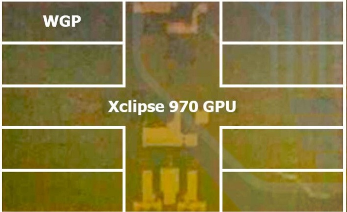
SemiAnalysis has published what it describes as an exclusive first look at Samsung's Exynos 2700, the smartphone SoC expected to arrive in 2027 using Samsung Foundry's SF2P process. The leaked die shot outlines a layout with a large NPU block, 24 MB of SLC, and an Xclipse 970 GPU with eight WGPs, the same WGP count as the Exynos 2600's Xclipse 960. As with the Exynos 2600, the modem remains a separate component rather than being integrated into the SoC.
A revised CPU core layout
The most notable change is on the CPU side. SemiAnalysis's CPU IP annotations and assumptions have been corrected by X user Piglin (@Shulker1024). Samsung appears to be doubling its prime (Ultra) core count to two for this generation, joining a trend that is now widespread across the industry. Apple has used two prime cores for years, Qualcomm has done so since the original Snapdragon 8 Elite, and Xiaomi's Xring O3 continues the dual prime setup already present in its O1 predecessor. The leaked Dimensity 9600 Pro would mark MediaTek's first use of two prime cores, while the upcoming Snapdragon 8 Elite Gen 6 Extreme likely continues Qualcomm's existing approach. The Exynos 2700 pairs two different Arm core families rather than using two matching prime cores. One prime and middle core pairing uses Arm's C1-Ultra (3.36 GHz) and four C1-Pro cores (2.88 GHz), while the other uses Arm's C2-Ultra (4.24 GHz) and four C2-Pro cores (3.74 GHz), for a total of 10 CPU cores. Running the older C1 cores at a lower clock speed alongside the newer C2 cores at a higher clock speed suggests that Samsung is using C1 for sustained efficiency and C2 for peak performance rather than deploying two symmetric prime cores.
That dual prime core approach addresses a structural issue that hardware analysis channel Geekerwan found in the Exynos 2600's 1+9 cores layout. Unlike its competitors, the Exynos 2600 has only a single prime core and nine middle cores, with no intermediate "big" core tier to bridge the gap. When CPU demand exceeded what the lower clocked C1-Pro cores could handle but did not require the C1-Ultra, Samsung had to clock three of the middle cores up to 3.25 GHz to compensate, pushing them well outside their efficient operating range and consuming disproportionate amounts of power. A second, lower clocked prime core on the Exynos 2700 would give the scheduler a clearer high performance option before it has to use the largest core.
Fixing the GPU bandwidth bottleneck
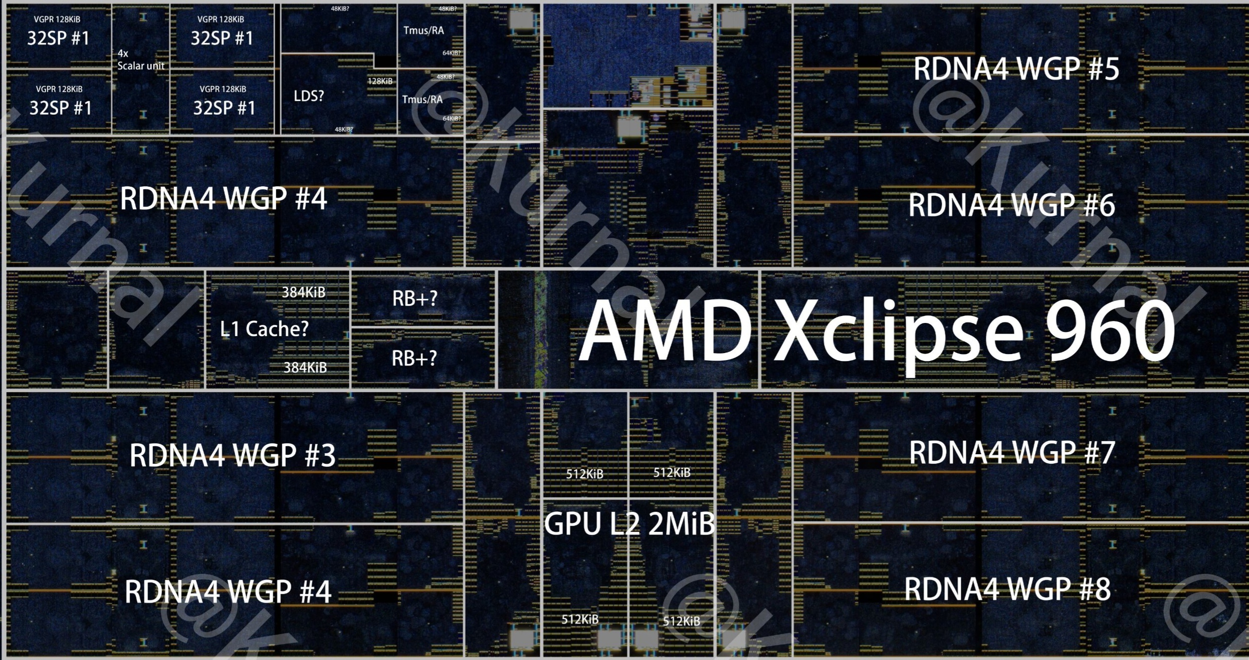
LPDDR6 support also appears to be confirmed by the die's PHY layout, raising the SoC's memory-bandwidth ceiling. That matters because the Exynos 2600's Xclipse 960 GPU was previously found to be bandwidth constrained rather than compute constrained. According to Geekerwan, the Xclipse 960 occupied roughly 23% of the Exynos 2600's total die area around 46% more than Qualcomm's Adreno GPU in a comparable SoC and offered roughly 7 TFLOPS of theoretical throughput. With mobile LPDDR bandwidth capping out at more than 80 GB/s and only 2 MB of GPU L2 cache onboard, Geekerwan's analysis found that the GPU regularly hit a memory wall under bandwidth heavy workloads, leaving compute resources idle while waiting for memory.
Whether Samsung has increased the Xclipse 970's GPU L2 cache beyond that 2 MB figure remains unconfirmed in the SemiAnalysis leak, but there are signs pointing in that direction. The proportion of the GPU block occupied by the eight WGPs appears visually smaller relative to the total GPU die area than it does on the Exynos 2600's Xclipse 960. This suggests that Samsung may have allocated more of the GPU footprint to uncore logic in this generation, including L2 cache and other supporting blocks such as raster and cache coherency interfaces. No die measurements were provided for the GPU block, and the image's resolution is not high enough to estimate the actual L2 capacity from its area alone. Still, the apparent shift in proportions is a reasonable indication that the uncore area and potentially the L2 cache has grown. If that translates into a larger GPU L2 cache, it could help alleviate the memory bottleneck Geekerwan found in the Exynos 2600, alongside the additional external bandwidth provided by LPDDR6. Still, as with all coverage of engineering samples and pre-launch leaks, these specifications are subject to change before devices powered by the Exynos 2700 reach retail.
Source(s)
SemiAnalyis, Piglin, Kurnal (via X), Geekerwan
 Add as a preferred source on Google


