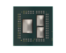
The range of SoCs based on the freshest version of AMD's latest design is still yet to be formally released. Nevertheless, the company has already indicated that it could be linked to an approximately 30% gain on performance compared to the last generation under certain conditions. This is because this generation, Zen 2, is based on a 7-nanometer (nm) architecture, whereas its predecessor, Zen+, was associated with a 12nm design.
As exceptional an advance Zen 2 may well be, it is possible that its eventual next generation, Zen 3, will be even better. This iteration of AMD's silicon will also be 7nm. However, it will be produced using the improved extreme UV lithography (EUV) method. A new report has indicated that this packs many more transistors into a comparable space - up to 20%, in fact.
This improved density should have a positive impact on the instructions per clock (IPC) count associated with Zen 3, even compared to Zen 2. Nevertheless, the improved EUV-derived structure may also result in power-consumption improvements of up to 10%. Accordingly, these chips are to be called 7nm+, rather than the more basic 7nm.
However, these prospects are reserved for the farther-flung future, whereas Zen 2 is very nearly part of the one we live in. New releases set to incorporate it include Ryzen 3000-based GPUs; next-generation Threadrippers and the potentially impressive, disruptive server-grade EPYC Rome CPUs.


