

Intel Core Ultra 7 265U vs Intel Core i9-14900 vs Intel Core Ultra 7 255U
Intel Core Ultra 7 265U
► remove from comparisonThe Intel Core Ultra 7 265U is an upper mid-range CPU with 12 cores from the Arrow Lake U series, which was introduced at the beginning of 2025. The SoC is based on a tile/chiplet design. The chip is similar to the Meteor Lake U series, but the compute part is manufactured using the modern Intel 3 process and therefore offers higher clock rates.
The smaller compute tile (compared to the H processors) offers 2 performance cores (P cores, Redwood Cove architecture, SMT) and 8 efficiency cores (E cores, Crestmont architecture). The P-cores support hyperthreading (therefore 14 threads together) and clock up to 5.3 GHz. The E-cores clock at a maximum of 4.2 GHz. In addition, there are now two more low-power efficiency cores on the low-power island, so the compute tile can be completely deactivated when idle and during simple tasks in order to save power.
Performance
Thanks to the significantly higher clock rates, the Core Ultra 7 265U should be significantly faster than the old Core Ultra 7 165U (12 cores, max 4.9 / 3.8 GHz, 12 MB cache). Due to the 12 cores, the multi-thread performance is very good, but can be limited by the low TDP (especially under long load).
Graphics unit
The Core Ultra 7 265U offers a new Arc-based iGPU called Intel Graphics with 4 Xe cores and 64 EUs that reach a maximum of 2.1 GHz. However, the performance is clearly below the new Arc iGPU in the H series.
Features
Arrow Lake-U has integrated WiFi 6E (WiFi 7 optional) and Thunderbolt 4 (4x). The integrated memory controller now supports LPDDR5/x-8400 or DDR5-6400 (max. 128 GB). A dedicated NPU (2x Gen3 Neural Compute Engines) is now used. The Xe Media Engine supports MPEG-2, AVC, VC-1 Decode, JPEG, VP8 Decode, VP9, HEVC and AV1 Decode up to 8K 10-bit HDR. The chip now supports PCIe-5.0 (x8 for GPU) and PCIe-4.0 (three x12 for SSDs).
Power consumption
The Intel Core Ultra 7 265U is specified with 15 watts TDP (base) and 57 watts (PL2) max. turbo power. Meteor Lake consists of five individual chips, whereby the processor part is manufactured in the new Intel 3 process (5nm). The graphics unit is produced at TSMC in N5 and the SoC and I/O tile in the older N6 process. These 4 chips are then applied to the 22nm base tile using the Foveros process.
Intel Core i9-14900
► remove from comparison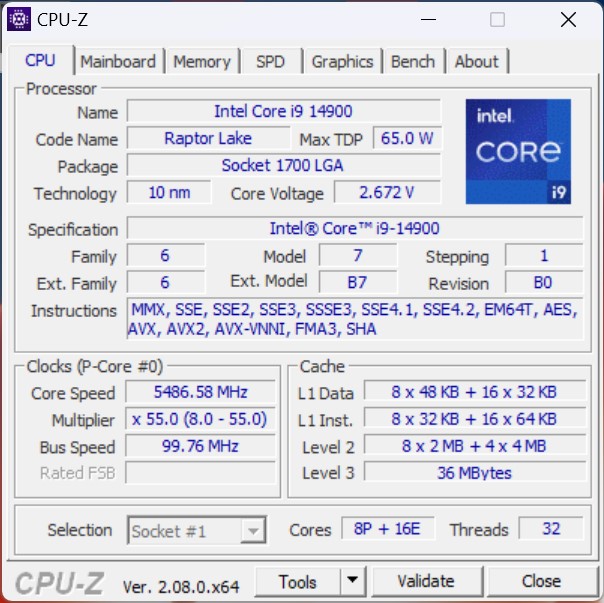
The Intel Core i9-14900 is a high-end processor based on the Raptor Lake architecture. The base clock is 2 GHz and can reach up to 5.8 GHz under optimal conditions. Similar to the top model (Intel Core i9-14900K), the total of 32 threads are divided into 8 p- and 16 e-cores. The 8 performance cores (p-cores) also offer hyperthreading, which means that a total of 32 threads can be processed simultaneously. The non-K model is an economical processor. There is still the option of DDR4 or DDR5 memory.
Performance
Compared to the Intel Core i9-14900K, the Core i9-14900 offers the same number of physical computing units. However, due to the lower power consumption, the Intel Core i9-14900 delivers slightly less performance. The intended use is primarily for compact PCs with limited cooling options.
Graphics unit
Like the Intel Core i9-14900K, the Intel Core i9-14900 offers an integrated graphics unit. The Intel Iris Xe architecture continues to serve as the basis. In terms of performance, however, nothing has changed with the Intel UHD Graphics 770.
Power consumption
The Intel Core i9-14900 is specified with a TDP of 65 watts, which corresponds to the PL1 value. In boost mode, the processor's performance can increase to up to 219 watts (PL2). However, this requires very good cooling. Compared to the Intel Core i9-13900, the specified power consumption has not changed.
Intel Core Ultra 7 255U
► remove from comparisonThe Intel Core Ultra 7 255U is an upper mid-range CPU with 12 cores from the Arrow Lake U series, which was introduced at the beginning of 2025. The chip is similar to the Meteor Lake U series, but the compute part is manufactured using the modern Intel 3 process and therefore offers higher clock rates.
Like its predecessor, the SoC is based on a tile/chiplet design. The smaller compute tile (compared to the H processors) offers 2 performance cores (P cores, Redwood Cove architecture, SMT) and 8 efficiency cores (E cores, Crestmont architecture). The P-cores support hyperthreading (therefore 14 threads together) and clock up to 5.2 GHz. The E-cores clock at a maximum of 4.2 GHz. In addition, there are now two more low-power efficiency cores with up to 2.4 GHz on the low-power island; the compute tile can therefore be completely deactivated when idle and during simple tasks in order to save power.
Performance
Due to the higher clock rates, the Core Ultra 7 255U can clearly distinguish itself from the old top model Core Ultra 7 165U (12 cores, max 4.9 / 3.8 GHz, 12 MB cache). The old Core Ultra 7 155U lags even further behind due to its low clock rates.
Graphics unit
The Core Ultra 7 155U offers a new Arc-based iGPU called Intel Graphics with 4 Xe cores and 64 EUs that reach a maximum of 2.1 GHz. However, the performance is far below the new Arc iGPU in the H series.
Features
Arrow Lake-U has integrated WiFi 6E (WiFi 7 optional). The integrated memory controller now supports LPDDR5/x-8400 or DDR5-6400 (max. 128 GB). A dedicated NPU (2x Gen3 Neural Compute Engines) is now used. The Xe Media Engine supports MPEG-2, AVC, VC-1 Decode, JPEG, VP8 Decode, VP9, HEVC and AV1 Decode up to 8K 10-bit HDR. The chip now supports PCIe-5.0 (x8 for GPU) and PCIe-4.0 (three x12 for SSDs).
Power consumption
The Intel Core Ultra 7 255U is specified with 15 watts TDP (base) and 57 watts (PL2) max. turbo power. Meteor Lake consists of five individual chips, whereby the processor part is manufactured in the new Intel 3 process (5nm). The graphics unit is produced at TSMC in N5 and the SoC and I/O tile in the older N6 process. These 4 chips are then applied to the 22nm base tile using the Foveros process.
| Model | Intel Core Ultra 7 265U | Intel Core i9-14900 | Intel Core Ultra 7 255U | ||||||||||||||||||||||||||||||||||||||||||||||||||||||||||||
| Codename | Arrow Lake-U | Raptor Lake | Arrow Lake-U | ||||||||||||||||||||||||||||||||||||||||||||||||||||||||||||
| Series | Intel Meteor Lake-U | Intel Raptor Lake-R | Intel Meteor Lake-U | ||||||||||||||||||||||||||||||||||||||||||||||||||||||||||||
| Series: Meteor Lake-U Arrow Lake-U |
|
|
| ||||||||||||||||||||||||||||||||||||||||||||||||||||||||||||
| Clock | 2400 - 5300 MHz | 2000 - 5800 MHz | 3800 - 4800 MHz | ||||||||||||||||||||||||||||||||||||||||||||||||||||||||||||
| L3 Cache | 12 MB | 36 MB | 12 MB | ||||||||||||||||||||||||||||||||||||||||||||||||||||||||||||
| Cores / Threads | 12 / 14 2 x 5.3 GHz Intel Redwood Cove P-Core 8 x 4.2 GHz Intel Crestmont E-Core 2 x 2.1 GHz Intel Crestmont E-Core | 24 / 32 8 x 5.8 GHz Intel Raptor Cove P-Core 16 x 4.3 GHz Intel Gracemont E-Core | 12 / 14 2 x 5.2 GHz Intel Redwood Cove P-Core 8 x 4.2 GHz Intel Crestmont E-Core 2 x 2.4 GHz Intel Crestmont E-Core | ||||||||||||||||||||||||||||||||||||||||||||||||||||||||||||
| TDP | 15 Watt | 65 Watt | 15 Watt | ||||||||||||||||||||||||||||||||||||||||||||||||||||||||||||
| TDP Turbo PL2 | 57 Watt | 219 Watt | |||||||||||||||||||||||||||||||||||||||||||||||||||||||||||||
| Technology | 5 nm | 10 nm | 5 nm | ||||||||||||||||||||||||||||||||||||||||||||||||||||||||||||
| max. Temp. | 110 °C | 100 °C | 110 °C | ||||||||||||||||||||||||||||||||||||||||||||||||||||||||||||
| Features | DDR5-6400/LPDDR5-8400/LPDDR5x-8400 RAM, PCIe 4, Thread Director, DL Boost, AI Boost, vPro Enterp., RPE, MMX, SSE, SSE2, SSE3, SSSE3, SSE4.1, SSE4.2, AES, AVX, AVX2, AVX-VNNI, FMA3, SHA | DDR5-6400/LPDDR5-8400/LPDDR5x-8400 RAM, PCIe 4, Thr. Director, DL Boost, AI Boost, vPro Essen., MMX, SSE, SSE2, SSE3, SSSE3, SSE4.1, SSE4.2, AES, AVX, AVX2, AVX-VNNI, FMA3, SHA | |||||||||||||||||||||||||||||||||||||||||||||||||||||||||||||
| iGPU | Intel Graphics 4-Core iGPU (Arc) ( - 2100 MHz) | Intel UHD Graphics 770 (300 - 1650 MHz) | Intel Graphics 4-Core iGPU (Arc) ( - 2100 MHz) | ||||||||||||||||||||||||||||||||||||||||||||||||||||||||||||
| Architecture | x86 | x86 | x86 | ||||||||||||||||||||||||||||||||||||||||||||||||||||||||||||
| Announced | |||||||||||||||||||||||||||||||||||||||||||||||||||||||||||||||
| Manufacturer | ark.intel.com | www.intel.de | ark.intel.com | ||||||||||||||||||||||||||||||||||||||||||||||||||||||||||||
| L2 Cache | 32 MB | ||||||||||||||||||||||||||||||||||||||||||||||||||||||||||||||
| Die Size | 257 mm2 | ||||||||||||||||||||||||||||||||||||||||||||||||||||||||||||||
| Socket | LGA 1700 | BGA2049 | |||||||||||||||||||||||||||||||||||||||||||||||||||||||||||||
| $549 U.S. |

Benchmarks
Average Benchmarks Intel Core i9-14900 → 0% n=0
* Smaller numbers mean a higher performance
1 This benchmark is not used for the average calculation