Samsung starts mass producing 14nm EUV DDR5 DRAM
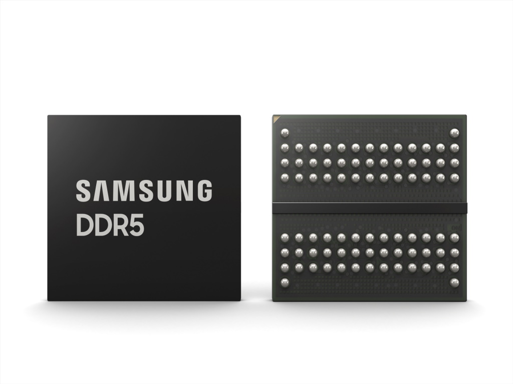
Samsung has announced that it has started mass production of the state-of-the-art 14nm, EUV-based DDR5 DRAM. Samsung also announced that the company has managed to increase the EUV layer count to five. This has allowed the Korean giant to get the highest DRAM bit density in the market, while also improving the wafer productivity by 20%. Furthermore, due to the use of the 14nm fabrication process, Samsung’s new DDR5 DRAM chips are up to 20% more power efficient as compared to the company’s previous generation DRAM node.
According to Jooyoung Lee, Samsung Electronics Senior Vice President and Head of DRAM Product & Technology, Samsung’s multi-layered EUV makes 14nm DDR5 DRAM possible, a product that wasn’t on the cards with the traditional argon fluoride (ArF) process.
Samsung’s newly developed DDR5 DRAM will run at speeds nearing 7.2 gigabits per second (Gbps), nearly double the DDR4 speeds. This will provide a significant speed boost to server applications and AI workloads. Samsung is also looking to grow the bit density of its 14nm DDR5 offerings to 24Gb in the coming years, further cementing the company as the go-to semiconductor manufacturer in the AI and 5G space.
Source(s)
