Rumor | Samsung 3nm GAAFET mass production will kick off by the end of June 2022 at the earliest
Samsung has been said to have been trailing TSMC in terms of getting new chips based on 3nm architectures to potential clients such as Qualcomm or AMD. However, according to the latest rumors, it might just be the other way around, as the South Korean behemoth might be in a position to officially launch the necessary production nodes as early as the coming week (June 27-July 3, 2022).
The vice-chairman of Samsung's Electronics division, Lee Jae-yong, has reportedly approached the chip-making equipment firm ASML in an attempt to strengthen ties with that potentially crucial partner ahead of plans to scale 3nm wafer production using the Dutch firm's extreme ultraviolet (EUV) lithography tech up to mass production capacity.
Furthermore, Samsung has reportedly presented Joe Biden with a 3nm demo during the US President's official May 2022 South Korea visit. The company reportedly intends to make its next-gen chips (which may form the basis of processors such as the rumored Apple M2 Pro and Ryzen 8000 series) based on the MBCFET structure.
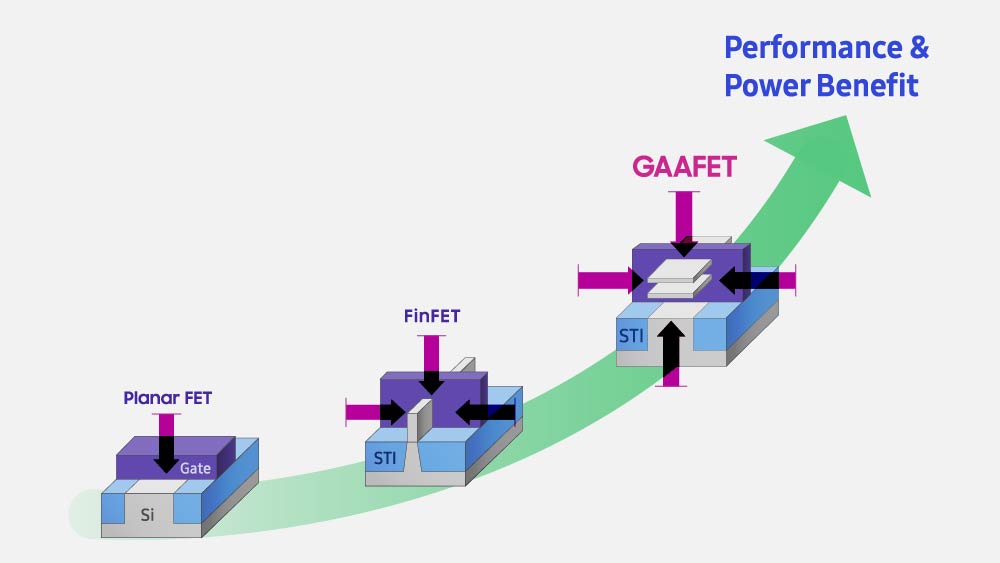
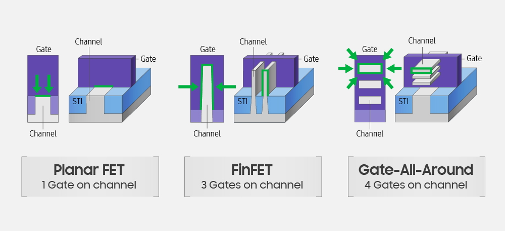
The "Multi-Bridge Channel Field Effect Transistor" is Samsung's patented take on the GAAFET, rated to improve on the more traditional FinFET in that each individual transistor's silicon channel (or channels, as in newer examples) is surrounded by gate electrode material on all 4 sides.
This (according to Samsung, at least) allows for the generational reduction of operational voltage, leading to proportional increases in power-efficiency and semiconductor performance. In the case of the MBCFET, the channels can also become wider within the gate material, thanks to a revolutionary nanosheet (as opposed to nanowire) production process.
This should (in theory) allow for more channel surface area in contact with that of the gate, and, thus, enhanced exposure to current. TSMC, on the other hand, is slated to stick with FinFET for its 3nm chips.
Nevertheless, it still commands over 50% of the semiconductor market share in 2022, compared to Samsung's ~16%. The latter might hope that its ongoing up-to-US$150 billion investment drive can help it get back on top by the time 3nm becomes the top-end standard in processing hardware.
Source(s)
