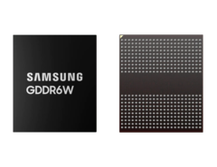
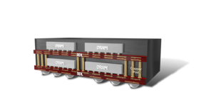
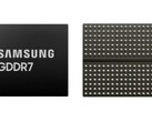
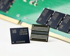
Samsung announces the GDDR6W specs less than 2 months after it introduced the GDDR7 specs. It looks like products integrating the GDDR7 VRAM chips might take a while longer to hit the market, as Samsung claims that the JEDEC standardization for GDDR6W VRAM products has already been completed in Q2 of this year, and the South Korean giant is planning to bring this standard to notebooks and the high performance computing sector as soon as possible. Besides offering higher bandwidth plus double the capacity and I/O pins over the 24 Gbps GDDR6X chips, the GDDR6W standard is developed with the revolutionary FOWLP (fan-out wafer-level packaging) design that allows for an unchanged footprint so that integrators can use the same production process from GDDR6X and reduce implementation time and costs.
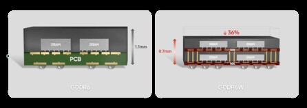
The capacity is now doubled from 16 Gb to 32 Gb per die, while the I/O pin oount doubled from 32 to 64. This not only translates to a 50% area reduction over GDDR6X, but the FOWLP also reduces the height of the die from 1.1 mm to 0.7 mm by eliminating the PCB base layer and replacing it with a silicon wafer that integrates VRAM chips itself.
As far as raw bandwidth is concerned, Samsung says the GDDR6W VRAM can almost match the HBM standard in a more efficient way. While the HBM2E chips have a system-level bandwidth of 1.6 TB/s with 4096 I/O pins and 3.2 Gbps transfer rate per pin, the new GDDR6W standard offers 1.4 TB/s bandwidth with 512 I/O pins and a 22 Gbps rate per pin. Reducing the number of I/O lanes by 8 times essentially eliminates the need for an interposer layer and makes it more cost-effective for product integrators. For reference, GDDR6X offers up to 1.1 TB/s bandwidth, so GDDR6W would be ~30% faster. On the other hand, GDDR7 is expected to offer 1.7 TB/s bandwidth over a 384-bit bus.


