

AMD Ryzen 5 8640HS vs Intel Pentium 8500 vs Intel Core i3-1210U
AMD Ryzen 5 8640HS
► remove from comparison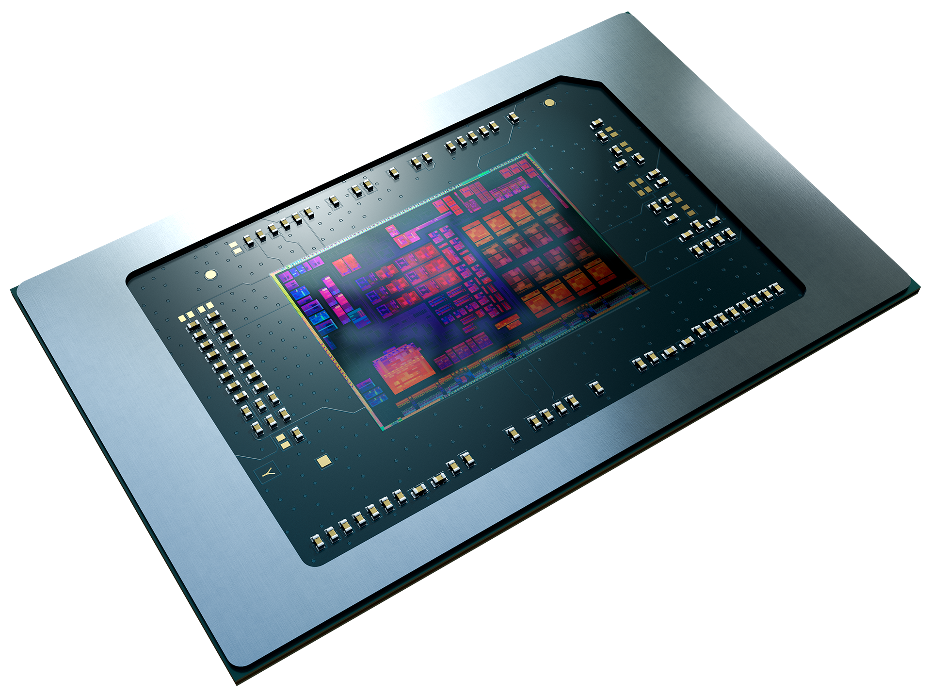
The Ryzen 5 8640HS is a mid-range, Hawk Point family processor that was unveiled in Q4 2023. The 8640HS isn't actually a new chip; instead, it's a rebadged Ryzen 5 7640U with a slightly higher wattage as well as higher clock speeds on the Ryzen AI NPU. The 8640HS has 6 SMT-enabled cores (12 threads) running at 3.5 GHz to 4.9 GHz. Those Zen 4 architecture cores are mated to the Radeon 760M integrated graphics adapter.
Architecture & Features
Hawk Point chips are powered by the Zen 4 architecture, much like Phoenix and Dragon Range family chips are. That's not to say there is no difference between the three. With Hawk Point, AMD is betting big on generative AI; these processors are set to deliver an up to 40% increase in generative AI performance over 7040 series APUs.
Unlike Zen 3, Zen 4 features AVX512 support and, thanks to a plethora of other improvements including larger caches/registers/buffers, is slated to deliver a double-digit IPC improvement over the former.
Elsewhere, the 8640HS has 16 MB of L3 cache and USB 4 support (therefore, Thunderbolt is supported as well). The chip is compatible with DDR5-5600 and LPDDR5x-7500 RAM which is still impressive as of late 2023.
A system powered by this Ryzen 5 will have access to twenty PCIe 4 lanes; this means a speedy enough NVMe SSD will be able to deliver speeds up to 7.8 GB/s.
Systems powered by this APU are expected to run 64-bit Windows 11, 64-bit Windows 10, or Linux. Like most laptop chips, the 8640HS is neither overclockable nor user-replaceable. It gets soldered to the motherboard for good (FP7, FP7r2, FP8 socket interfaces).
Performance
It's safe to expect the APU to be at least 15% faster than the Zen 3 Plus-powered Ryzen 5 6600U (6 cores, 12 threads, up to 4.5 GHz), as far as multi-thread performance is concerned.
Your mileage may vary depending on how high the CPU power limits are and how competent the cooling solution of your laptop is.
Graphics
The Radeon 760M has 8 CUs (512 shaders) running at up to 2,600 MHz. While not great for gaming (unless you are fine with resolutions such as 900p and low detail settings), the iGPU will let you use up to 4 monitors with resolutions as high as SUHD 4320p. It also HW-decodes and HW-encodes the most widely used video codecs including AV1, HEVC, AVC without breaking a sweat.
Power consumption
The 8640HS has a long-term power limit (default TDP) of 28 W that laptop makers are free to change to anything between 20 W and 30 W. Most companies will probably go for a higher value to get better performance. Either way, an active cooling solution is a must for any system powered by the chip.
Last but not the least, the 8640HS is manufactured on TSMC's 4 nm process for high, as of late 2023, energy efficiency.
Intel Pentium 8500
► remove from comparisonThe Intel Pentium 8500 is an entry-level low-power mobile CPU for thin and light laptops based on the Alder Lake architecture. It was announced in early 2022 and offers one performance core (P-cores, Golden Cove architecture) and 4 efficient cores (E-cores, Gracemont architecture). The P-cores support Hyper-Threading leading to 6 supported threads when combined with the E-cores. The clock rate ranges from 1 to 4.4 GHz on the performance cluster and 0.7 to 3.3 GHz on the efficient cluster. The performance of the E-cores should be similar to old Skylake cores (compare to the Core i7-6700HQ). All cores can use up to 8 MB L3-cache. Compared to the faster Core i3-1210U, the Pentium offers one less P-core.
Performance
While we have not tested a single system built around the 8500 as of August 2023, it's safe to expect the chip to be about 20% slower than the i3-1215U, as far as multi-thread performance is concerned. Which is pretty terrible as of Q3 2023.
Your mileage may vary depending on how high the CPU power limits are and how competent the cooling solution of your system is.
Features
The integrated memory controller supports various memory types up to DDR5-4800, DDR4-3200, LPDDR5-5200, and LPDDR4x-4267. The Thread Director (in hardware) can support the operating system to decide which thread to use on the performance or efficient cores for the best performance. For AI tasks, the CPU also integrates GNA 3.0 and DL Boost (via AVX2). Quick Sync in version 8 is the same as in the Rocket Lake CPUs and supports MPEG-2, AVC, VC-1 decode, JPEG, VP8 decode, VP9, HEVC, and AV1 decode in hardware. The CPU only supports PCIe 4.0 (x8 for a GPU and two x4 for SSDs).
The integrated graphics adapter is based on the Xe-architecture and offers 48 of the 96 EUs (Execution Units) operating at up to 0.8 GHz.
Power consumption
This Pentium has a Base power consumption of 9 W, with 29 W being its maximum Intel-recommended Turbo power consumption. TDP values this low allow for passively cooled laptops, tablets, mini-PCs as long as performance is not a priority.
The CPU is made with Intel's 3rd generation 10 nm process marketed as Intel 7 for decent, as of early 2023, energy efficiency.
Intel Core i3-1210U
► remove from comparisonThe Intel Core i3-1210U is a low power mobile CPU for thin and light laptops based on the Alder Lake architecture. It was announced in early 2022 and offers 2 performance cores (P-cores, Golden Cove architecture) and 4 efficient cores (E-cores, Gracemont architecture). The P-cores support Hyper-Threading leading to 8 supported threads when combined with the E-cores. The clock rate ranges from 1 to 4.4 GHz on the performance cluster and 0.7 to 3.3 GHz on the efficient cluster. The performance of the E-cores should be similar to old Skylake cores (compare to the Core i7-6700HQ). All cores can use up to 10 MB L3 cache.
Performance
While we have not tested a single system built around the 1210U as of August 2023, we fully expect its multi-thread performance to be pretty much identical to that of the i3-1215U. Which is pretty fast for an entry-level chip, as of mid 2023.
Your mileage may vary depending on how high the CPU power limits are and how competent the cooling solution of your system is.
Features
The integrated memory controller supports various memory types up to DDR5-4800, DDR4-3200, LPDDR5-5200, and LPDDR4x-4267. The Thread Director (in hardware) can support the operating system to decide which thread to use on the performance or efficient cores for the best performance. For AI tasks, the CPU also integrates GNA 3.0 and DL Boost (via AVX2). Quick Sync in version 8 is the same as in the Rocket Lake CPUs and supports MPEG-2, AVC, VC-1 decode, JPEG, VP8 decode, VP9, HEVC, and AV1 decode in hardware. The CPU only supports PCIe 4.0 (x8 for a GPU and two x4 for SSDs).
The integrated graphics adapter is based on the Xe-architecture and offers 64 of the 96 EUs (Execution Units) operating at up to 0.9 GHz.
Power consumption
This Core i3 has a Base power consumption of 9 W, with 29 W being its maximum Intel-recommended Turbo power consumption. TDP values that low allow for passively designs as long as performance is not a priority.
The CPU is built with Intel's 3rd generation 10 nm process marketed as Intel 7 for decent, as of early 2023, energy efficiency.
| Model | AMD Ryzen 5 8640HS | Intel Pentium 8500 | Intel Core i3-1210U | ||||||||||||||||||||||||||||||||||||||||||||||||||||||||||||||||||||||||||||||||||||||||||||||||||||||||||||||||||||||||||||||||||||||||||||||||||||||||||||||||
| Codename | Hawk Point-HS (Zen 4) | Alder Lake-U | Alder Lake-U | ||||||||||||||||||||||||||||||||||||||||||||||||||||||||||||||||||||||||||||||||||||||||||||||||||||||||||||||||||||||||||||||||||||||||||||||||||||||||||||||||
| Series | AMD Hawk Point (Zen 4/4c) | Intel Alder Lake-M | Intel Alder Lake-M | ||||||||||||||||||||||||||||||||||||||||||||||||||||||||||||||||||||||||||||||||||||||||||||||||||||||||||||||||||||||||||||||||||||||||||||||||||||||||||||||||
| Series: Alder Lake-M Alder Lake-U |
|
|
| ||||||||||||||||||||||||||||||||||||||||||||||||||||||||||||||||||||||||||||||||||||||||||||||||||||||||||||||||||||||||||||||||||||||||||||||||||||||||||||||||
| Clock | 3500 - 4900 MHz | 700 - 4400 MHz | 700 - 4400 MHz | ||||||||||||||||||||||||||||||||||||||||||||||||||||||||||||||||||||||||||||||||||||||||||||||||||||||||||||||||||||||||||||||||||||||||||||||||||||||||||||||||
| L1 Cache | 384 KB | 464 KB | 544 KB | ||||||||||||||||||||||||||||||||||||||||||||||||||||||||||||||||||||||||||||||||||||||||||||||||||||||||||||||||||||||||||||||||||||||||||||||||||||||||||||||||
| L2 Cache | 6 MB | 3.5 MB | 5 MB | ||||||||||||||||||||||||||||||||||||||||||||||||||||||||||||||||||||||||||||||||||||||||||||||||||||||||||||||||||||||||||||||||||||||||||||||||||||||||||||||||
| L3 Cache | 16 MB | 8 MB | 10 MB | ||||||||||||||||||||||||||||||||||||||||||||||||||||||||||||||||||||||||||||||||||||||||||||||||||||||||||||||||||||||||||||||||||||||||||||||||||||||||||||||||
| Cores / Threads | 6 / 12 6 x 4.9 GHz AMD Zen 4 | 5 / 6 | 6 / 8 | ||||||||||||||||||||||||||||||||||||||||||||||||||||||||||||||||||||||||||||||||||||||||||||||||||||||||||||||||||||||||||||||||||||||||||||||||||||||||||||||||
| TDP | 28 Watt | 9 Watt | 9 Watt | ||||||||||||||||||||||||||||||||||||||||||||||||||||||||||||||||||||||||||||||||||||||||||||||||||||||||||||||||||||||||||||||||||||||||||||||||||||||||||||||||
| Technology | 4 nm | 10 nm | 10 nm | ||||||||||||||||||||||||||||||||||||||||||||||||||||||||||||||||||||||||||||||||||||||||||||||||||||||||||||||||||||||||||||||||||||||||||||||||||||||||||||||||
| Die Size | 178 mm2 | ||||||||||||||||||||||||||||||||||||||||||||||||||||||||||||||||||||||||||||||||||||||||||||||||||||||||||||||||||||||||||||||||||||||||||||||||||||||||||||||||||
| max. Temp. | 100 °C | 100 °C | 100 °C | ||||||||||||||||||||||||||||||||||||||||||||||||||||||||||||||||||||||||||||||||||||||||||||||||||||||||||||||||||||||||||||||||||||||||||||||||||||||||||||||||
| Socket | FP7/FP7r2/FP8 | BGA1744 | BGA1744 | ||||||||||||||||||||||||||||||||||||||||||||||||||||||||||||||||||||||||||||||||||||||||||||||||||||||||||||||||||||||||||||||||||||||||||||||||||||||||||||||||
| Features | DDR5-5600/LPDDR5x-7500 RAM, PCIe 4, Ryzen AI, AES, AVX, AVX2, AVX512, FMA3, MMX (+), SHA, SSE, SSE2, SSE3, SSE4.1, SSE4.2, SSE4A, SSSE3 | LPDDR4x-4266/LPDDR5-5200 RAM, PCIe 4, Thr. Director, DL Boost, GNA, MMX, SSE, SSE2, SSE3, SSSE3, SSE4.1, SSE4.2, AES, AVX, AVX2, FMA3, SHA | LPDDR4x-4266/LPDDR5-5200 RAM, PCIe 4, Thr. Director, DL Boost, GNA, MMX, SSE, SSE2, SSE3, SSSE3, SSE4.1, SSE4.2, AES, AVX, AVX2, FMA3, SHA | ||||||||||||||||||||||||||||||||||||||||||||||||||||||||||||||||||||||||||||||||||||||||||||||||||||||||||||||||||||||||||||||||||||||||||||||||||||||||||||||||
| iGPU | AMD Radeon 760M ( - 2600 MHz) | Intel UHD Graphics Xe G4 48EUs ( - 800 MHz) | Intel UHD Graphics 64EUs (Alder Lake 12th Gen) ( - 850 MHz) | ||||||||||||||||||||||||||||||||||||||||||||||||||||||||||||||||||||||||||||||||||||||||||||||||||||||||||||||||||||||||||||||||||||||||||||||||||||||||||||||||
| Architecture | x86 | x86 | x86 | ||||||||||||||||||||||||||||||||||||||||||||||||||||||||||||||||||||||||||||||||||||||||||||||||||||||||||||||||||||||||||||||||||||||||||||||||||||||||||||||||
| Announced | |||||||||||||||||||||||||||||||||||||||||||||||||||||||||||||||||||||||||||||||||||||||||||||||||||||||||||||||||||||||||||||||||||||||||||||||||||||||||||||||||||
| Manufacturer | www.amd.com | ark.intel.com | ark.intel.com |

Benchmarks

Average Benchmarks AMD Ryzen 5 8640HS → 0% n=0
Average Benchmarks Intel Pentium 8500 → 0% n=0
* Smaller numbers mean a higher performance
1 This benchmark is not used for the average calculation