TSMC to introduce intermediary 6 nm EUV-based node
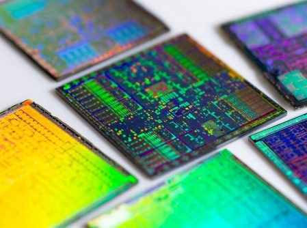
Even though TSMC already entered risk production for the 5 nm node, the company recently announced that it will also ready a 6 nm node that will expand on the EUV lithography introduce for the 7 nm+ node. The intermediary node will have design rules fully compatible with the current 7 nm node, offering a seamless migration path and fast design cycle.
TSMC’s 6 nm node is expected to deliver 18% higher logic density over the original 7 nm node. The company does not, however, mention the benefits over the new 7 nm EUV node. Risk production for the 6 nm node is scheduled for Q1 2020, so almost one year after the 5 nm risk production, which could mean that TSMC is not going to focus too much on this technology.
Samsung finished the development of its 5 nm node, and TSMC is most likely looking to make the jump to its own 5 nm node as soon as possible, in order to further maintain its transistor density leadership for a broad array of applications including high-to-mid end mobile, consumer applications, AI, networking, 5G infrastructure, GPU, and high-performance computing. TSMC also announced that the development for the 3 nm node is under way and production could start before 2022.
Meanwhile, Intel is still struggling to release its first 10 nm CPUs, but these models are said to have transistor densities similar to the upcoming 7 nm CPUs from AMD, so technically, Intel is not that far behind.
TSMC Unveils 6-nanometer Process |
7-nanometer Enhancement Combines Performance/Cost Advantage with Fast Time-to-Market |
Issued by: TSMC Issued on: 2019/04/16 |
| Hsinchu, Taiwan, R.O.C. – April 16, 2019 - TSMC (TWSE: 2330, NYSE: TSM) today announced its 6-nanometer (N6) process, which provides a significant enhancement of its industry-leading N7 technology and offers customers a highly competitive performance-to-cost advantage as well as fast time-to-market with direct migration from N7-based designs. By leveraging the new capabilities in extreme ultraviolet (EUV) lithography gained from the N7+ technology currently in risk production, TSMC’s N6 process delivers 18% higher logic density over the N7 process. At the same time, its design rules are fully compatible with TSMC’s proven N7 technology, allowing its comprehensive design ecosystem to be reused. As a result, it offers a seamless migration path with a fast design cycle time with very limited engineering resources for customers to achieve the product benefits from the new technology offering. Scheduled for risk production in the first quarter of 2020, TSMC’s N6 technology provides customers with additional cost-effective benefits while extending the industry-leading power and performance from the 7nm family for a broad array of applications, ranging from high-to-mid end mobile, consumer applications, AI, networking, 5G infrastructure, GPU, and high-performance computing. “TSMC N6 technology will further extend our leadership in delivering product benefits with higher performance and cost advantage beyond the current N7,” said Dr. Kevin Zhang, TSMC Vice President of Business Development. “Building upon the broad success of our 7nm technology, we’re confident that our customers will be able to quickly extract even higher product value from the new offering by leveraging a well-established design ecosystem today.” |
