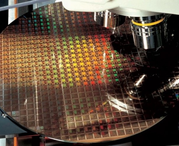
Samsung releases roadmap to 3 nm fabrication process
On May 22, Samsung disclosed a detailed manufacturing process milestone roadmap for the next several years at the company’s 3rd annual US Samsung Foundry Forum. The South Korean company is determined to deliver the fastest and most energy-efficient SoCs for high-performance computing and connected devices that would “give people access to data, analysis and insight in new and previously unthought-of ways to make human lives better.” Samsung included an overview of its next major stepping milestones all the way up to 3 nm.
Just like TSMC’s tech, Samsung’s 7 nm stepping (called 7 nm Low Power Plus) will be using the extreme ultra-violet lithography solution for improved energy efficiency and decreased die size. It is scheduled to be in full production mode by 2H 2018, with key IPs (i.e. the Exynos 9820 SoC) already under development and expected to launch in early 2019.
Next up is the 5 nm stepping (5 nm Low Power Early), which should further improve the area scaling and reduced energy requirements brought by the 7 nm stepping. As expected, there is no mention of increased processing power at this level.
Immediately after that, Samsung will release the 4 nm Low Power/Plus stepping, which will be the last milestone to use the current FinFet semiconductor tech. Samsung will make sure that this stepping can provide an easy migration to the next gen semiconductor tech brought by the following stepping.
Last but not least, the 3 nm Gate-All-Around Early/Pus introduced the GAA next gen semiconductor tech. In order to overcome the physical scaling and performance limitations derived from the already venerable FinFET tech, Samsung is currently developing the next gen MBCFET (Multi-Bridge-Channel FET) that uses a nano-sheet device. Starting with the 3 nm stepping, the overall performance will see significant improvements.
Samsung did not mention any timeline for the 5 nm and 4 nm stepping, but the 3 nm stepping is expected to be released by 2022.
Source(s)
