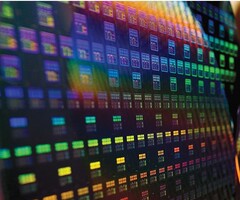
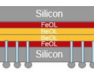
TSMC is currently rolling out the first batch of 7 nm chips for some companies like AMD and memory chip manufacturers like Micron and Cadence. While these chips will be commercialized later this year, it is important to note that the first wave of 7 nm products does not use the upgraded extreme ultraviolet (EUV) lithography, which is scheduled to be implemented by late 2018. So the first wave of 7 nm chips will see significant performance gains, but the power consumption will not be on par with the theoretical yields, at least not until TSMC implements the new EUV tech. Later down the road, around 2020, TSMC expects to shift to the 5 nm process, which will itself rely on improved EUV tech.
Speaking of the 5 nm stepping, TSMC revealed that the improved EUV lithography should greatly increase the transistor density, but, since there is a mere 2 nm difference from the 7 nm process, the performance and power improvements will be quite negligible.
According to TSMC’s estimates, the improvements brought by the 7+ nm stepping should see 30% increased performance stats, 50% decreased power requirements and 54% reduced area when compared to the 10 nm stepping. However, when comparing the 7+ nm stepping to the 5 nm one, the power consumption should only see 20% improvements and a mere 15% performance gain, but at least the area will be reduced by 45%.
Regarding the EUV lithography availability, TSMC stated that the daily power levels for the special light sources are currently hitting 145 W, but they need to reach 300 W for maximum efficiency, and this will happen later this year. The first 7 nm chips using the full-fledged EUV tech will roll out in early 2019.
Loading Comments
I first stepped into the wondrous IT&C world when I was around seven years old. I was instantly fascinated by computerized graphics, whether they were from games or 3D applications like 3D Max. I'm also an avid reader of science fiction, an astrophysics aficionado, and a crypto geek. I started writing PC-related articles for Softpedia and a few blogs back in 2006. I joined the Notebookcheck team in the summer of 2017 and am currently a senior tech writer mostly covering processor, GPU, and laptop news.
> Expert Reviews and News on Laptops, Smartphones and Tech Innovations > News > News Archive > Newsarchive 2018 05 > TSMC reveals more details on the 5 nm manufacturing process
Bogdan Solca, 2018-05- 9 (Update: 2026-02-18)


