AMD and Nvidia future GPUs could integrate TSMC's new wafer-on-wafer tech
The 3D NAND memory chips found in present day SSDs already make use of something generally known as stacking. This technology may also be implemented in future CPUs, and, if TSMC manages to convince AMD/Nvidia, it could also be used in upcoming GPUs. On May 1st, Taiwan Semiconductor Manufacturing Company reevaled the wafer-on-wafer manufacturing technique during a symposium held in Santa Clara, California, also announcing a partnership with Cadence, which will be able to manufacture 5 nm and 7+ nm mobile chips using the aforementioned stacking technology.
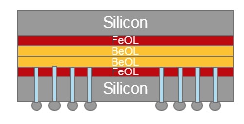
Instead of one wafer per chip, future GPUs may include two or more wafers stacked vertically, which would double the performance without the need to develop new horizontal designs every 2 years. A dual wafer setup, for example, would be achieved by flipping the upper wafer over the lower one, binding both via a flip-chip package. Thus, future GPUs could include multiple wafers in one die and the operating system could detect it as a multi-processor graphics card, eliminating the need for SLI setups.
One shortcoming for this technology would be its lower manufacturing yields for sizes lower than 16 nm. If one of the stacked wafers does not pass the QA, the entire stack is discarded, leading to low yields and poor cost effectiveness. TSMC is currently working to improve this technology so that sub-12 nm processes could equally benefit from it.
AMD and Nvidia could take advantage of this technology in the sense of launch one generation with a single wafer, then, for the next few years, they could be adding one or two more wafers per core, effectively doubling the performance without working on the architecture at all. This would give them more time to work on revolutionary architectures meanwhile.
Source(s)
