AMD Ryzen 7 9700X vs AMD Ryzen 9 H 270 vs AMD Ryzen 5 240
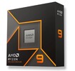
AMD Ryzen 7 9700X
► remove from comparison
The AMD Ryzen 7 9700X is an upper mid-range desktop CPU of the Granite Ridge product family that sports 8 Zen 5 cores (16 threads) running at 3.8 GHz to 5.5 GHz, along with PCIe 5 support and a basic RDNA 2 architecture iGPU. The Ryzen was launched in June 2024, with sales slated to start some time in August.
Architecture and Features
Like Strix Point APUs, Granite Ridge processors make use of the new Zen 5 microarchitecture. However, there are no efficient cores here; all of 9700X's cores are full Zen 5 cores with a "proper" Zen 5 implementation, not the simplified mobile version that has a lower AVX-512 performance. Furthermore, Granite Ridge is a multi-die design with only the CPU cores produced using a fairly modern 4 nm TSMC process. Strix Point processors are a single-die design, from what we know.
According to AMD, desktop Zen 5 delivers a 16% IPC uplift over Zen 4 thanks to branch prediction improvements and other refinements.
Elsewhere, the 9700X has 32 MB of L3 cache and 24 direct PCIe 5 lanes (3.93 GB/s throughput per lane) with up to 12 additional PCIe 4 lanes available depending on the motherboard. It supports DDR5 RAM as fast as 5,600 MT/s (up to 8,000 MT/s if overclocked).
The 9700X is unlocked for overclocking. Naturally, the AM5 socket CPU fully supports Windows 11, 64-bit Windows 10 as well as many Linux distros.
Performance
In our review, the Ryzen 7 delivered multi-thread benchmark scores very close to those of the Ryzen AI 9 HX 370 and 375, as well as the Core i7-12700 and i7-12700K.
Graphics
The Radeon 610M comes equipped with just 128 unified shaders running at up to 2,200 MHz. While this certainly isn't a gaming GPU, it's fast enough to run some competitive titles such as Counter-Strike 2 (~50 fps at 1080p / Low) as well as older (pre-2019) titles.
It can HW-decode many popular video codecs including first and foremost AVC, HEVC, VP9, AV1.
Power consumption
The CPU cores are built with TSMC's N4P process for a good, as of mid 2024, power efficiency. (Apple is the leader in this regard with the second-generation 3 nm process.)
The Ryzen 7's long-term TDP is either 65 W or 105 W, with each user free to make their own choice. If overclocked, its power consumption figures will increase significantly.
AMD Ryzen 9 H 270
► remove from comparison
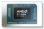
The Ryzen 9 H 270 is a rebadged Ryzen 9 270 (or Ryzen 9 8945HS) for China, making it a fast mobile laptop processor. This is an APU of the Hawk Point family that has eight Zen 4 cores running at 4.0 GHz to 5.2 GHz. This APU was introduced at CES 2025 and all of its cores are SMT-enabled for a total of 16 processing threads.
Architecture and Features
Hawk Point family chips are powered by the Zen 4 architecture, much like Phoenix and Dragon Range family chips were. The 16 TOPS NPU present here isn't powerful enough for systems built around the 9 270 to be Copilot+ certified.
Elsewhere, the chip has 16 MB of L3 cache and support for super-fast DDR5-5600 and LPDDR5x-7500 RAM while also being compatible with USB 4 and thus with Thunderbolt. It comes with 20 PCIe 4 lanes, giving fast NVMe SSD up to 7.8 GB/s of throughput.
Please note that this processor is not overclockable and neither is it user-replaceable. It gets soldered to the motherboard for good instead (FP8 socket interface).
Performance
Its CPU performance is slated to be identical to the old Ryzen 9 8945HS and R9 7940HS.
Your mileage may vary depending on how high the CPU power limits are and how competent the cooling solution of your system is.
Graphics
The Radeon 780M has 12 CUs (768 shaders) purring away at up to 2,800 MHz. The Radeon will let you use up to 4 monitors with resolutions as high as SUHD 4320p and it will also HW-decode and HW-encode the most widely used video codecs (such as AV1, HEVC and AVC) without breaking a sweat. As for gaming, most 2024 games run fine at 1080p with settings set to Low on this graphics adapter.
Your mileage may vary depending on how high the CPU power limits are, how competent the cooling solution of the system is, how fast the RAM of the system is (there is no dedicated VRAM here).
Power consumption
This Ryzen 9 series chip has a long-term power limit (default TDP) of 35 W to 54 W, giving laptop makers a choice between longer battery life and higher performance. Either way, an active cooling solution is a must for a system powered by this chip.
The R9 H 270 is built with TSMC's 4 nm process for a reasonably good, as of early 2025, energy efficiency.
AMD Ryzen 5 240
► remove from comparison
The Ryzen 5 240 is an upper mid-range processor (APU) of the Hawk Point family. This isn't an entirely new chip, but a rebadged Ryzen 5 8645HS from 2024. The CPU features 6 SMT-enabled Zen 4 cores (12 threads) running at 4.3 GHz to 5.0 GHz. The Radeon 760M iGPU is responsible for carrying out 3D calculations and similar duties.
Architecture & Features
Hawk Point family chips are powered by the Zen 4 architecture, much like Phoenix and Dragon Range family chips are. That's not to say there is no difference between the three. With Hawk Point, AMD is betting big on generative AI; these chips are promised to deliver an up to 40% increase in generative AI performance over 7040 series APUs making apps like DaVinci Resolve and Adobe Photoshop even more powerful.
Unlike Zen 3, Zen 4 features AVX512 support and, thanks to a plethora of other improvements including larger caches/registers/buffers across the board, is slated to bring a double-digit IPC improvement over the former.
Elsewhere, the R5 240 has 16 MB of L3 cache and a super-fast DDR5-5600 / LPDDR5x-7500 RAM controller. USB 4 (and thus Thunderbolt) is supported natively and so is PCIe 4. In fact, 20 PCIe 4 lanes are on offer; data transfer speeds of up to 7.8 GB/s will be possible provided a sufficiently fast NVMe SSD is used.
Systems powered by this Ryzen 5 series chip are expected to run 64-bit Windows 11, 64-bit Windows 10, or Linux. Please note that the APU is not overclockable and neither will you be able to replace it with a faster one as it gets soldered to the motherboard permanently (FP7, FP7r2, FP8 socket interfaces).
Performance
Since the Ryzen 5 240 is an 8645HX / 7640HS in disguise, it is safe to expect the APU to be about as fast as the Ryzen 9 5900HX, Ryzen 7 6800H, Ryzen 7 7736U and also the Core i5-12500H, as far as multi-thread performance is concerned.
Your mileage may vary depending on how high the CPU power limits are and how competent the cooling solution of your system is.
Graphics
The Radeon 760M has 8 CUs (512 shaders) running at up to 2,600 MHz. While this is not the best graphics adapter for gaming as it's only just fast enough for low quality settings and resolutions such as 1600 x 900, it will let you connect up to four SUHD 4320p monitors and it also HW-encodes and HW-decodes the most widely used video codecs such as AV1, HEVC and AVC without breaking a sweat.
Power consumption
The Ryzen 5 240 has a long-term power limit (default TDP) of 35 W to 54 W, giving laptop makers a choice between improving battery life and giving the system they are working on more oomph. Either way, an active cooling solution is a must for any system powered by the chip.
This Ryzen 5 series APU is built with TSMC's 4 nm process for high, as of late 2023, energy efficiency.
| Model | AMD Ryzen 7 9700X | AMD Ryzen 9 H 270 | AMD Ryzen 5 240 | ||||||||||||||||||||||||||||||||||||||||||||||||||||||||||||||||||||||||||||||||||||||||||||||||||||||||||||||||||||||||||||||||||||||||
| Codename | Granite Ridge | Hawk Point-HS (Zen 4) | Hawk Point-HS (Zen 4) | ||||||||||||||||||||||||||||||||||||||||||||||||||||||||||||||||||||||||||||||||||||||||||||||||||||||||||||||||||||||||||||||||||||||||
| Series | AMD Granite Ridge (Zen 5, AM5) | AMD Hawk Point (Zen 4/4c) | AMD Hawk Point (Zen 4/4c) | ||||||||||||||||||||||||||||||||||||||||||||||||||||||||||||||||||||||||||||||||||||||||||||||||||||||||||||||||||||||||||||||||||||||||
| Series: Hawk Point (Zen 4/4c) Hawk Point-HS (Zen 4) |
|
|
| ||||||||||||||||||||||||||||||||||||||||||||||||||||||||||||||||||||||||||||||||||||||||||||||||||||||||||||||||||||||||||||||||||||||||
| Clock | 3800 - 5500 MHz | 4000 - 5200 MHz | 4300 - 5000 MHz | ||||||||||||||||||||||||||||||||||||||||||||||||||||||||||||||||||||||||||||||||||||||||||||||||||||||||||||||||||||||||||||||||||||||||
| L1 Cache | 512 KB | 512 KB | 384 KB | ||||||||||||||||||||||||||||||||||||||||||||||||||||||||||||||||||||||||||||||||||||||||||||||||||||||||||||||||||||||||||||||||||||||||
| L2 Cache | 8 MB | 8 MB | 6 MB | ||||||||||||||||||||||||||||||||||||||||||||||||||||||||||||||||||||||||||||||||||||||||||||||||||||||||||||||||||||||||||||||||||||||||
| L3 Cache | 32 MB | 16 MB | 16 MB | ||||||||||||||||||||||||||||||||||||||||||||||||||||||||||||||||||||||||||||||||||||||||||||||||||||||||||||||||||||||||||||||||||||||||
| Cores / Threads | 8 / 16 8 x 5.5 GHz AMD Zen 5 | 8 / 16 8 x 5.2 GHz AMD Zen 4 | 6 / 12 6 x 5.0 GHz AMD Zen 4 | ||||||||||||||||||||||||||||||||||||||||||||||||||||||||||||||||||||||||||||||||||||||||||||||||||||||||||||||||||||||||||||||||||||||||
| TDP | 65 Watt | 45 Watt | 45 Watt | ||||||||||||||||||||||||||||||||||||||||||||||||||||||||||||||||||||||||||||||||||||||||||||||||||||||||||||||||||||||||||||||||||||||||
| Technology | 4 nm & 6 nm | 4 nm | 4 nm | ||||||||||||||||||||||||||||||||||||||||||||||||||||||||||||||||||||||||||||||||||||||||||||||||||||||||||||||||||||||||||||||||||||||||
| max. Temp. | 95 °C | 100 °C | 100 °C | ||||||||||||||||||||||||||||||||||||||||||||||||||||||||||||||||||||||||||||||||||||||||||||||||||||||||||||||||||||||||||||||||||||||||
| Socket | AM5 | FP8 | FP7/FP7r2/FP8 | ||||||||||||||||||||||||||||||||||||||||||||||||||||||||||||||||||||||||||||||||||||||||||||||||||||||||||||||||||||||||||||||||||||||||
| Features | DDR5-5600 RAM, PCIe 5 + PCIe 4, SMT, AES, AVX, AVX2, AVX512, FMA3, MMX (+), SHA, SSE, SSE2, SSE3, SSSE3, SSE4.1, SSE4.2, SSE4A | DDR5-5600/LPDDR5x-7500 RAM, PCIe 4, USB 4, Ryzen AI (16 TOPS), MMX, SSE, SSE2, SSE3, SSSE3, SSE4A, SSE4.1, SSE4.2, AVX, AVX2, AVX-512, BMI2, ABM, FMA, ADX, SMEP, SMAP, SMT, CPB, AES-NI, RDRAND, RDSEED, SHA, SME | DDR5-5600/LPDDR5x-7500 RAM, PCIe 4, Ryzen AI, AES, AVX, AVX2, AVX512, FMA3, MMX (+), SHA, SSE, SSE2, SSE3, SSE4.1, SSE4.2, SSE4A, SSSE3 | ||||||||||||||||||||||||||||||||||||||||||||||||||||||||||||||||||||||||||||||||||||||||||||||||||||||||||||||||||||||||||||||||||||||||
| iGPU | AMD Radeon 610M ( - 2200 MHz) | AMD Radeon 780M ( - 2800 MHz) | AMD Radeon 760M ( - 2600 MHz) | ||||||||||||||||||||||||||||||||||||||||||||||||||||||||||||||||||||||||||||||||||||||||||||||||||||||||||||||||||||||||||||||||||||||||
| Architecture | x86 | x86 | x86 | ||||||||||||||||||||||||||||||||||||||||||||||||||||||||||||||||||||||||||||||||||||||||||||||||||||||||||||||||||||||||||||||||||||||||
| Announced | |||||||||||||||||||||||||||||||||||||||||||||||||||||||||||||||||||||||||||||||||||||||||||||||||||||||||||||||||||||||||||||||||||||||||||
| Manufacturer | www.amd.com | www.amd.com | www.amd.com | ||||||||||||||||||||||||||||||||||||||||||||||||||||||||||||||||||||||||||||||||||||||||||||||||||||||||||||||||||||||||||||||||||||||||
| Die Size | 178 mm2 | 178 mm2 |
Benchmarks
Average Benchmarks AMD Ryzen 7 9700X → 0% n=0
Average Benchmarks AMD Ryzen 9 H 270 → 0% n=0
* Smaller numbers mean a higher performance
1 This benchmark is not used for the average calculation


