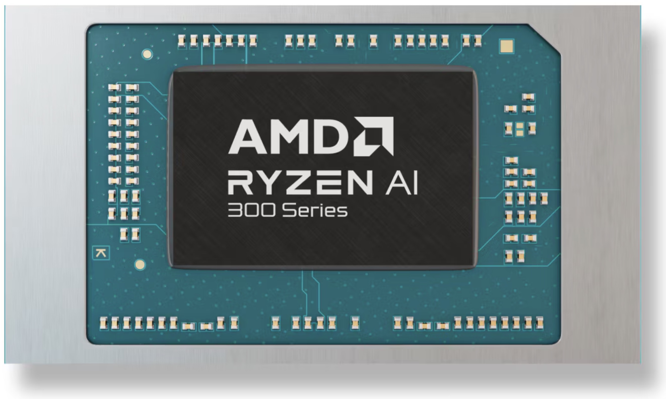
The AMD Ryzen AI 7 345 is a powerful mobile processor from the Krackan Point family. The APU integrates 6 CPU cores (2x Zen 5 with up to 4.6 GHz and 4x Zen 5c with less cache and a maximum of 3.4 GHz). The APU can only access 8 MB of L3 cache. The CPU was only introduced in mid-2026 and surprisingly offers weaker specifications (lower clock speeds, more Zen 5c cores instead of Zen 5 cores, and less L3 cache) than the older Ryzen AI 5 340 (6 cores, 4.8 GHz, 16 MB L3 cache).
Architecture and features
The APUs of the Krackan Point family use cores of the Zen 5 and Zen 5c microarchitectures, which are located in separate clusters. Zen 5c is a slightly slower, smaller and more energy-efficient version of Zen 5. One of the differences between Zen 5 and Zen 5c is the cache size; Zen 5 cores have larger caches.
However, the mobile Zen 5 implementation is reportedly (ChipsAndCheese) closer to desktop Zen 4 than desktop Zen 5 due to the different cache sizes, the large differences in AVX-512 throughput and other factors.
Otherwise, the Ryzen AI 7 chip supports DDR5-5600 and LPDDR5x-8000 RAM, allowing system designers to choose between lower latency and higher throughput. The chip is natively compatible with USB 4 (and therefore also with Thunderbolt). It has PCIe 4.0 support for a throughput of 1.9 GB/s per lane, just like its 8000 series predecessors. The integrated XDNA 2 NPU, which is significantly more complex than the first-generation XDNA, delivers up to 50 INT8 TOPS for accelerating various AI workloads.
As usual with laptop CPUs, the Ryzen AI 7 chip cannot be replaced by the user as it is soldered.
Performance
Due to the lower clock rates and smaller caches, performance should be slightly below that of the older AMD Ryzen AI 5 340 (6 cores, 4.8 GHz, 16 MB L3 cache).
Graphics
The Radeon 840M is a slimmed-down version of the 890M with only 4 CUs (= 256 shaders) and clocks at 2.9 GHz in the Ryzen AI 7 345. The iGPU uses the new RDNA 3.5 architecture.
Power consumption
The Ryzen AI 7 345 is said to have a base TDP of 28 W, although laptop manufacturers are free to set the TDP between 15 and 54 W.
The 4 nm process from TSMC, with which these CPUs are manufactured, ensures above-average energy efficiency.
Codename
Krackan Point (Zen 5)
Series
AMD Strix / Gorgon Point
Series: Strix / Gorgon Point Krackan Point (Zen 5)







 - Average benchmark values

 Add as a preferred source on Google


