Exclusive | NVIDIA Ampere RTX 30 Laptop GPUs: TGP woes apart, OEMs may also decide boost clocks on their own
Ever since NVIDIA officially announced the Ampere RTX 30 Laptop GPUs at CES 2021, there has been much consternation among members of the press and the public alike with NVIDIA's decision to not explicitly brand its laptop GPU offerings as Max-Q or otherwise. Though Max-Q itself still exists, it is now only an umbrella term to indicate the presence of technologies such as Advanced Optimus, Dynamic Boost 2.0 (DB 2.0) and WhisperMode 2.0.
With the RTX 30 Ampere Laptop GPUs, OEMs are free to decide on the cTGP and Max-Q features that they want. This can potentially cause a lot of confusion, especially for uninitiated buyers as they are likely to assume that a higher GPU model number automatically translated to higher performance whereas that need not always be the case.
Taking this into cognizance, we have published independent lists of laptops powered by each of the three Ampere laptop GPUs (linked below), and we are glad to see the good response. These lists would be updated whenever we get TGP and boost clock info directly form OEMs. However, we would like to have your attention to something important — those specifications may not necessarily be the real deal, even if official.
We are getting to know from our sources that NVIDIA has not shared any precise specifications with OEMs with respect to DB 2.0 values and associated clocks. Although NVIDIA on its part has clarified that it now requires OEMs to share power and clock information on their websites, we are hearing there is no clarity from NVIDIA as to what actually this information should be. This opens another can of worms as OEMs can now report boost clock info as they deem fit.
See also:
OEMs may not always indicate accurate boosts in spec sheets
Though NVIDIA says OEMs should mention the boost clocks for the corresponding TGP values, there are some inherent issues here. Firstly, OEMs can be expected to publicly declare only the maximum possible TGP. This is the sum of the base value, cTGP, and the applicable Dynamic Boost 2.0; the max TGP column in our tables also reflects the same.
So, a laptop with 110 W cTGP-up and 15 W Dynamic Boost 2.0 will likely indicate the total TGP as 125 W. Neither the driver nor third-party applications can actually separate these two power parameters for reasons we will come to shortly.
Secondly, even if an OEM does indicate a particular Dynamic Boost 2.0 value, there is no spec from NVIDIA detailing what can be the applicable boost clocks for the given DB 2.0 values; we are hearing that NVIDIA's tables only go up to base TGP without DB 2.0.
Therefore, the boost clocks for a particular cTGP+DB 2.0 combination can vary between OEMs.
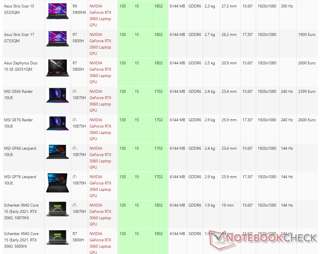
For instance, NVIDIA's official maximum boost clock for the RTX 3060 Laptop GPU is 1,703 MHz at 115 W base TGP. Now, all Asus and Schenker-XMG laptops featuring an RTX 3060 Laptop GPU with a maximum possible TGP of 130 W (115 W cTGP + 15 W DB 2.0) indicate the boost clock as 1,802 MHz. For the same max TGP values, however, MSI indicates the boost clock to be 1,702 MHz.
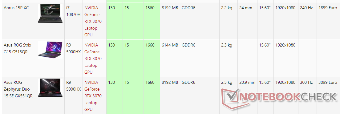
Similarly, in the case of a 130 W RTX 3070 Laptop GPU, we see that the Aorus 15P XC and Asus ROG SKus differ by 100 MHz boosts.
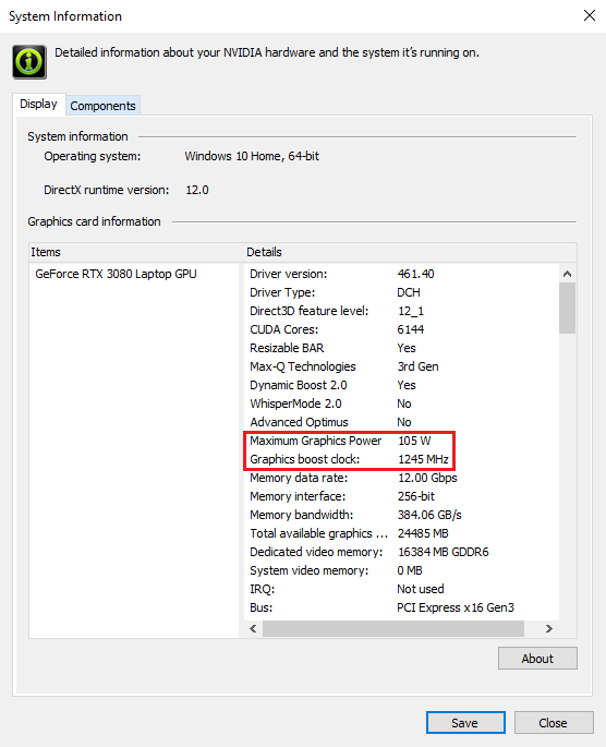
The NVIDIA driver isn't helpful in this regards either as it only reports the clocks pertaining to the baseline TGP. As illustrated in the screenshot below, the 105 W max TGP for the RTX 3080 Laptop GPU is the combined TGP+cTGP-up+DB 2.0 value whereas the indicated 1,245 MHz boost clock actually pertains only to the 80 W base TGP going by NVIDIA's official specifications.
Thus, even if the laptop can boost higher, the end user has no way of knowing it from the driver. The only way to know the full boost potential is to peruse independent reviews such as ours.
OEMs who go purely by NVIDIA's specs stand to lose out in the perception game compared to those who advertise a sort of "marked-up" boost clocks. The end user is at a disadvantage here because a purchasing decision cannot be made based on the advertised boost clocks.
Dynamic Boost 2.0 values are difficult to report
It is difficult to derive Dynamic Boost 2.0 values as the driver itself does not report them and neither can third-party utilities. Currently, this information can be had only from OEMs. This is because the actual real-world DB 2.0 values depend on many factors. DB 2.0 basically manages power allocated to the CPU, GPU, and the VRAM on a per-frame basis, so its extent depends largely on the workload and the leverage that the CPU provides not to forget the actual cooling mechanism itself and ambient temperature.
So, even if NVIDIA and OEMs say a particular RTX 3070 Laptop GPU, for example, offers up to 15 W DB 2.0, there is no guarantee that this will be attained in the real world. Ascertaining this via popular benchmarks such as 3DMark or FurMark is not exactly reliable and can lead to differences between reveiwers based on the parameters they select and how they also influence CPU load.
Why bother about such a variable, you ask? Because it affects the boost clock. The haughtily advertised boost clock may not be actually attainable simply because the limiting factor here is the extent of DB 2.0 that the GPU can leverage.
All said and done, the OEMs also need to be cut some slack here. Rather, NVIDIA should define and communicate to them (and to us) what is the expected boost for a given scenario. Better still, being able to split the TGP value components and displaying them in the driver — even if they are dynamic — helps the end user to get a fairly good idea of the kind of performance that can be expected from a particular configuration.
While OEMs have been doing their best to communicate these values to us, there is definitely more scope for a less-confusing method of estimating performance from the specs — just like the good ol' days.
Buy the Razer Blade 15 with Core i7-10750H and RTX 3060 on Amazon
Source(s)
Own
