Massive Nintendo Switch 2 leak reveals CPU/GPU specs and emulates real-world performance

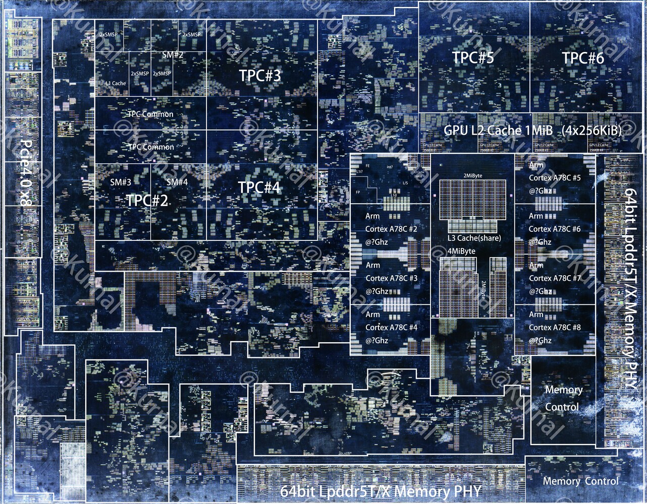
- Kurnalsalts, a well-known semiconductor teardown expert, has now shown us what powers the Nintendo Switch 2. We have a detailed die shot that shows us what makes its Tegra T239 chip tick. It has a die area of 207 mm2, making it nearly twice as large as the Nvidia chip found on the original Nintendo Switch. And contrary to our earlier report, it does not feature a tri-cluster CPU with a prime Cortex-X1 core.
Instead, it has eight Cortex-A78c cores working in tandem with each other. Their max clock speed is unknown at this point. For the GPU, it uses an Nvidia Ampere SKU, with 1,536 CUDA cores spread around 6 TPCs. It is manufactured on Samsung's 8N node, the same one used to make Ampere GPUs. This effectively debunks earlier claims of the Switch 2's T239 being a 5 nm die-shrunk version.
Geekerwan also tore down the Nintendo Switch 2 motherboard to reveal its important bits. For starters, it features two 6 GB LPDDR5X-8,533 modules from SK Hynix, running at a reduced clock rate. Its other components include a 256 GB SK Hynix UFS 3.1 module, Wi-Fi circuitry from MediaTek and a RealTek audio chip.
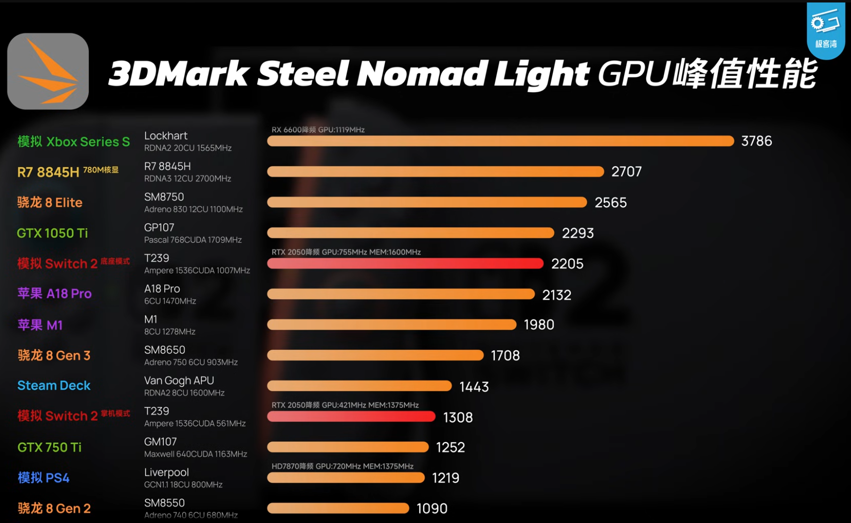
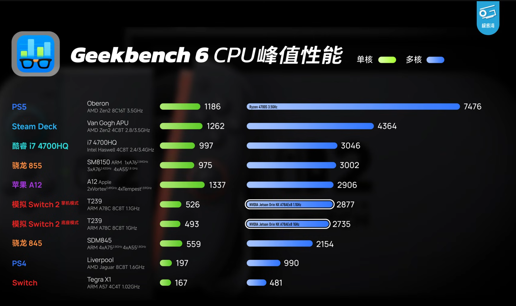
Given the Switch 2 is not out yet, it is hard to tell how it performs in the real world. Geekerwan tried to emulate it by underclocking a GeForce RTX 2050 laptop CPU, and found that the results lined up with performance numbers observed earlier. For example, Cyberpunk 2077 ran at 40 ish FPS with DLSS performance mode.
In synthetic benchmarks, the Nintendo Switch 2's GPU performs on par with a GeForce GTX 750 Ti from the yesteryears. On the CPU front, it trades blows with a six-gen old Apple A12. Of course, the tests have been performed on entirely different pieces of hardware and not the actual Switch 2.


Source(s)
