Patent shows future AMD RDNA-based GPUs could leverage multi-chip modules a la Intel Xe HP Arctic Sound and NVIDIA Hopper, but RDNA 3 will likely be monolithic
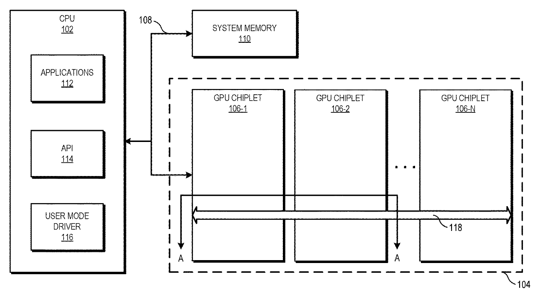
After having successfully demonstrated the efficacy of a multi-chip module design (MCM) on the CPU side, AMD may very well look forward to repeat the success on the GPU side of the equation as well. A patent titled "GPU Chiplets using High Bandwidth Crosslinks" filed in 2019 and now available on the Free Patents Online (FPO) website indicates that AMD does have some tricks up its sleeve to effectively transition from the conventional monolithic design.
The patent's abstract reads,
A chiplet system includes a central processing unit (CPU) communicably coupled to a first GPU chiplet of a GPU chiplet array. The GPU chiplet array includes the first GPU chiplet communicably coupled to the CPU via a bus and a second GPU chiplet communicably coupled to the first GPU chiplet via a passive crosslink. The passive crosslink is a passive interposer die dedicated for inter-chiplet communications and partitions systems-on-a-chip (SoC) functionality into smaller functional chiplet groupings."
In the patent application, AMD notes that monolithic dies are becoming expensive to manufacture. It also notes that parallel workloads in GPUs are difficult to properly distribute across multiple chiplets and keep memory across them in sync. Adding to this onerous task is that most applications are written keeping a single GPU in mind. Therefore, the challenge is to preserve the current programming model as much as possible while still offering a chiplet design to reduce manufacturing costs and improve yields.
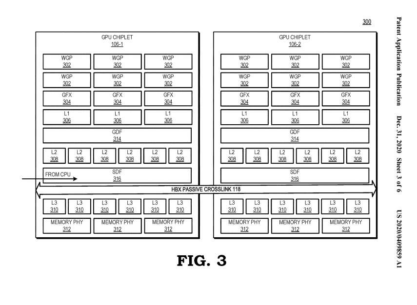
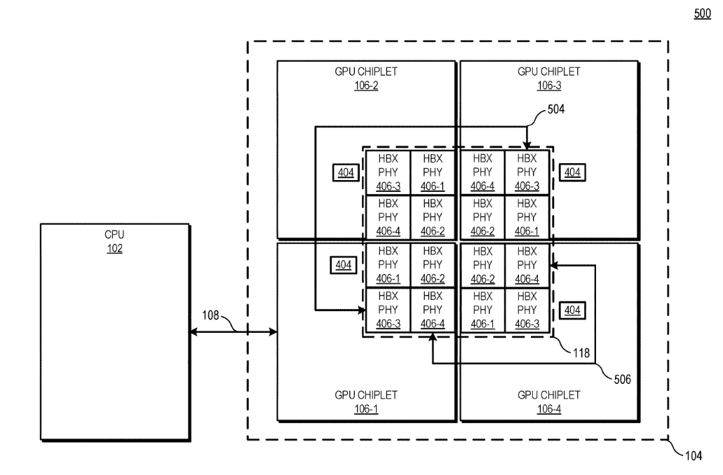
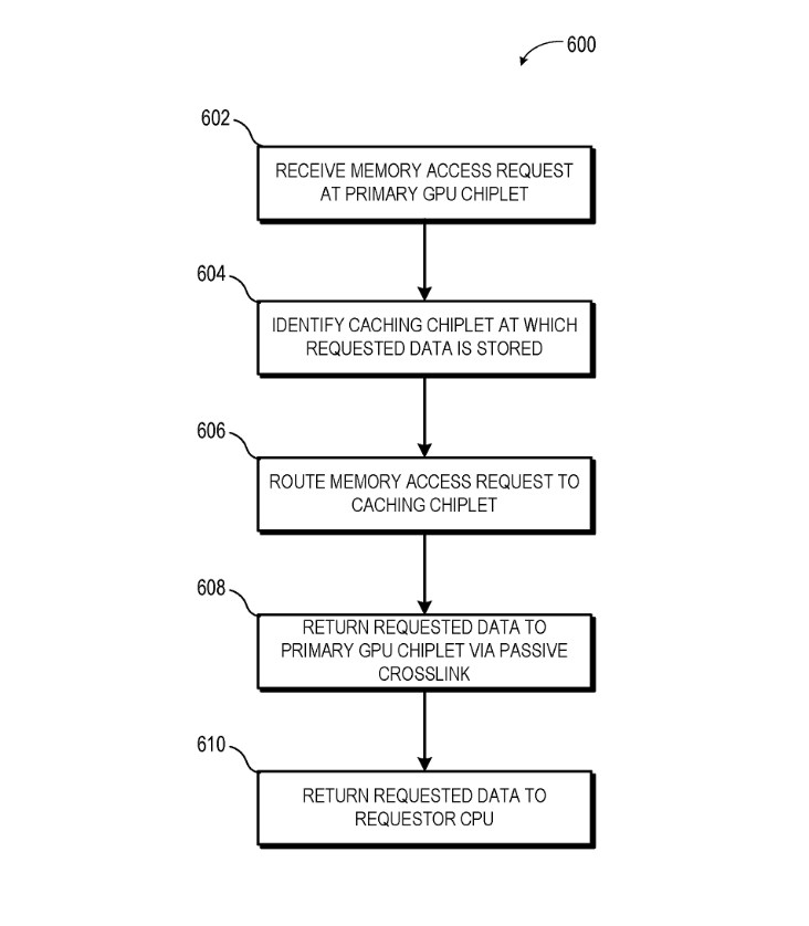
To overcome these concerns, AMD's patent envisages using the first GPU in the series of chiplets to directly couple to the CPU. The other GPU chiplets in the array would then be coupled to the primary GPU via a high-bandwidth passive crosslink (HBPC). The HBPC is essentially a passive interposer die dedicated for inter-chip communication across the SoC.
With regards to memory sync, the patent notes that though each GPU chiplet would feature its own last-level cache (LLC), all such LLCs are coupled in a way that enables coherency across all GPU chiplets. Since only the primary GPU chiplet receives requests from the CPU, the entire complex still appears monolithic to the CPU and consequently to the OS.
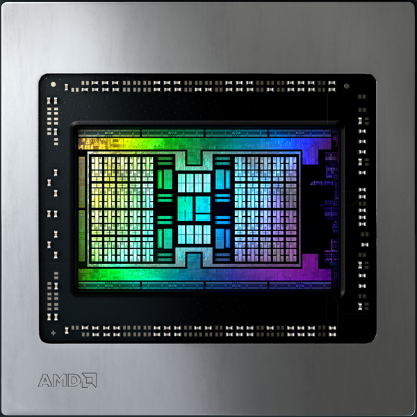
At the moment, AMD already offers multi-GPU designs on a single board. Previously, we have seen the AMD Radeon R9 295X2 and the Radeon Pro Duo. The newer Radeon Pro Vega II Duo is exclusive to the Apple Mac Pro and features two Radeon VIIs with 64 compute units (CUs) each connected by an Infinity Fabric link.
Back in 2018, AMD's SVP of Radeon Technologies Group (RTG) David Wang opined that unless a multi-GPU package is made invisible, ISVs may show some reluctance. However, he also expressed optimism that "anything's possible".
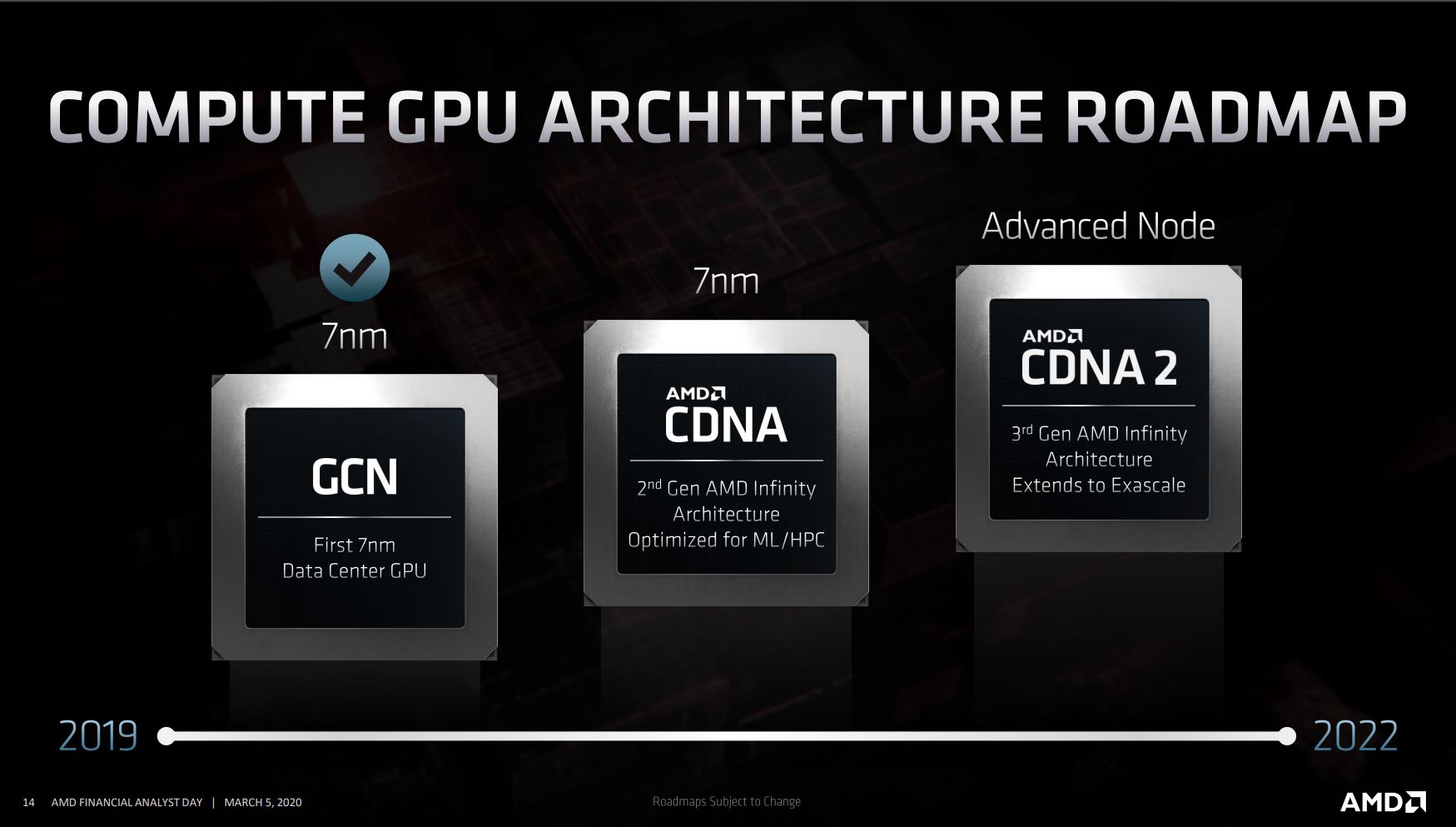
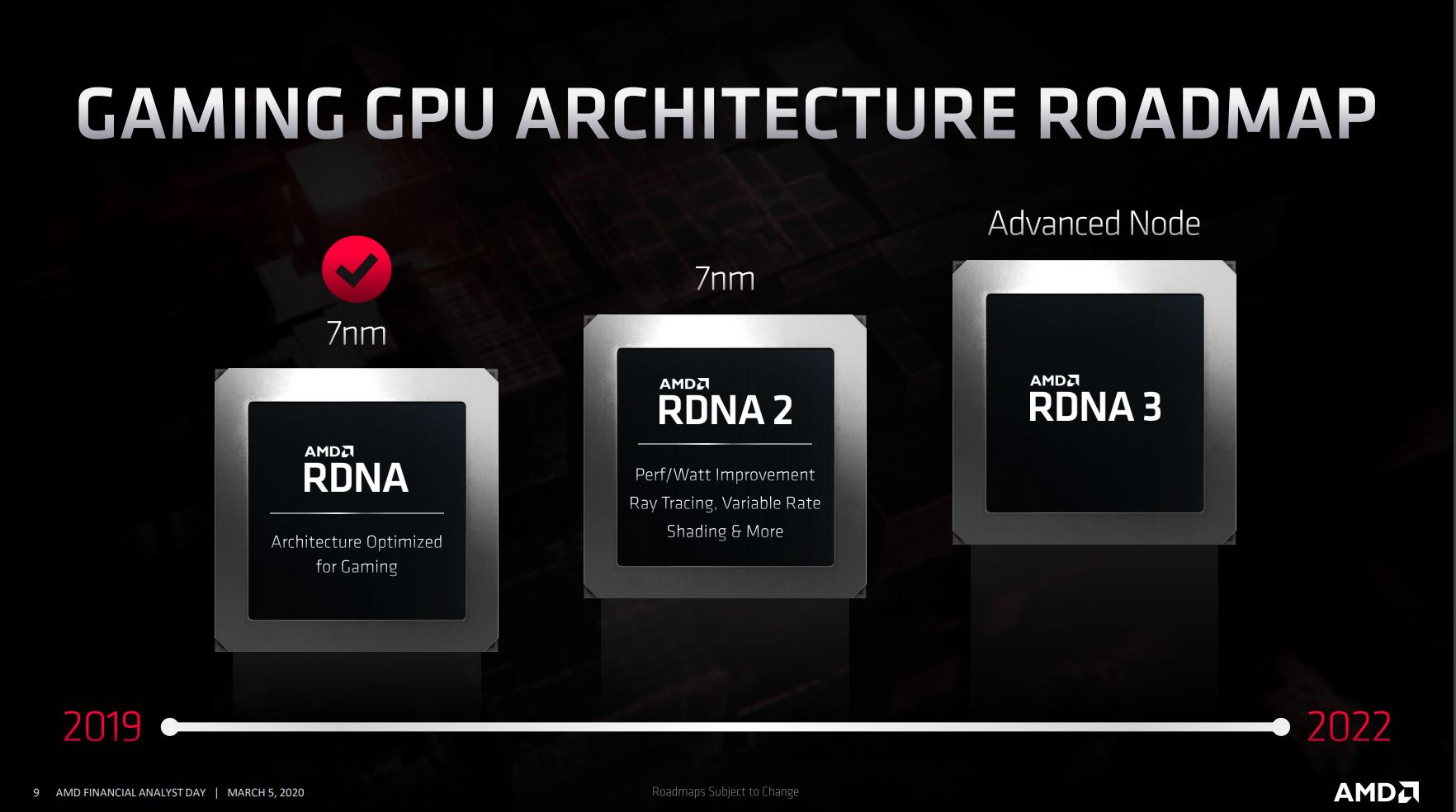
Now, it is not clear when we would see such a design in flesh. Official CDNA and RDNA roadmaps only point to an "Advanced Node" for 2022, so it is likely that we may not see CDNA 2 or RDNA 3 sporting multi-chip module (MCM) designs.
That being said, the competition is already showing similar trends with both Intel and NVIDIA looking to offer MCM parts with Xe HP Arctic Sound and Hopper, respectively.

Source(s)
