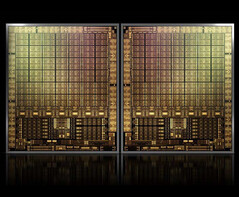
Nvidia Hopper is a name that has been rearing its head in the rumor mill once in a while for quite some time now. GH100 Hopper is slated to succeed GA100 Ampere and will be a high performance computing (HPC) focused card while its consumer counterpart is expected to be AD102 Lovelace. We had previously reported on the rumored die size of GH100, and we are now getting to know the probable transistor count.
This information comes via a poster Zhangzhonghao over at the Chiphell forums. The OP didn't actually mention GH100 or Hopper by name but posted, "140 billion+... is really scary, super nuclear bomb" (machine translated from Chinese). But it is not too hard to guess that he was pretty much referring to Nvidia's upcoming 5 nm HPC accelerator. If true, this rumored transistor count for Hopper is about 2.58x more than that of GA100 Ampere (54.2 billion) and 2.40x that of AMD Aldebaran Instinct MI200 (58.2 billion).
Recently, known leaker @kopite7kimi on Twitter claimed that GH100 Hopper could have a die area just short of 1000 mm2. However, the current lithography reticle limit of 858 mm2 makes his claim a bit hard to believe just yet. If somehow we do assume a 900 mm2 die area, GH100 Hopper could sport a massive 150 million transistors per mm2 on the 5 nm node. 3DCenter made some quick calculations and came up with numbers that indicate 486 or 972 million transistor per shading multiprocessor (144 SMs in total) depending on whether Hopper will have a "modest" 70 billion transistors or the 140 billion for real.
These numbers indicate that Hopper would likely be a multi-chip module (MCM) as has been speculated since long. However, recent rumors indicate that we will be seeing a monolithic die for the most part. It is not clear at this point whether Nvidia would be offering Hopper in both monolithic and MCM variants.
In a recent research paper published in the journal ACM Transactions on Architecture and Code Optimization, Nvidia brings up the issue of combining both FP16-based deep learning (DL) workloads and FP32 and above-based HPC workloads on a single GPU.
The paper postulates the benefits of a composable on-package GPU (COPA-GPU) architecture with an MCM design and also alludes to a mysterious GPU-N with 8,576 CUDA cores and 100 GB of HBM2 VRAM.
Nvidia has also referenced several designs with last-level cache (LLC) varying from 60 MB (in GPU-N) to 1,920 MB (in COPA-GPU 5) and RAM capacities ranging from 100 GB to 233 GB. Of course, most of this is theoretical, but it is possible that some of these variants will form part of the Hopper family.
We expect Nvidia to talk about GH100 Hopper during the company's GTC 2022 keynote on March 21.
Source(s)
Chiphell Forum (Chinese)


