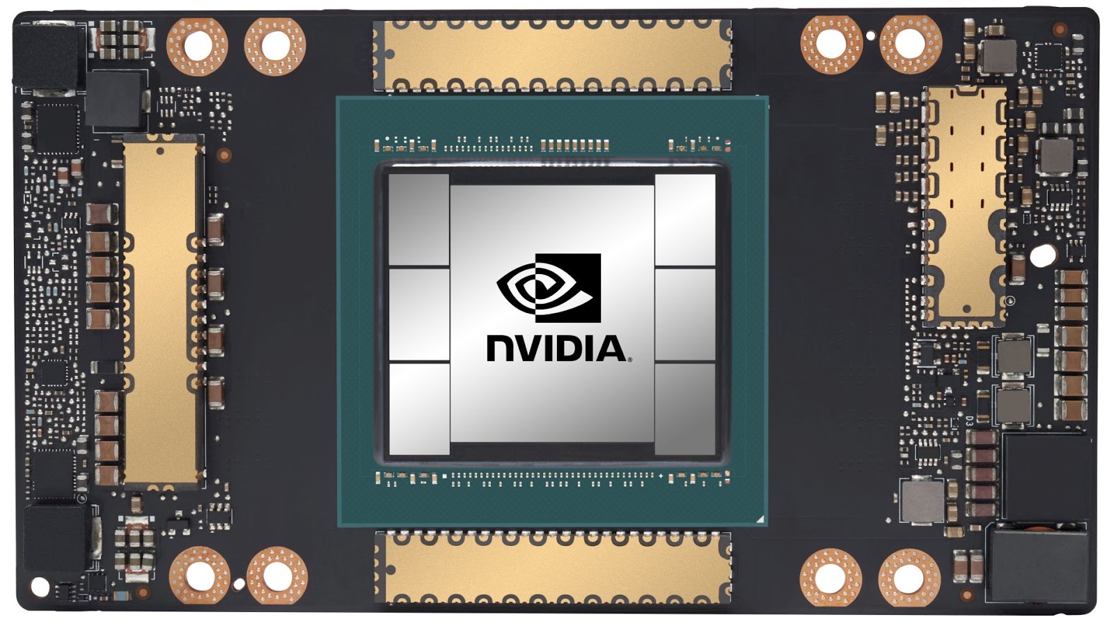
1000 W Nvidia Hopper GH100 rumored to be 21% larger than Ampere GA100, will be monolithic die contrary to popular perception
With the launch of the RTX 3090 Ti imminent, there is some chatter about what would the performance uplift be like from the original RTX 3090. Nvidia, meanwhile, is known to be already hard at work on Ampere's successor codenamed Lovelace AD102, which is expected to sport a massive 18,432 CUDA cores and possibly clocks north of 2.5 GHz. Information about Lovelace's contemporary, Hopper, has been quite scarce save for the fact that it is being targeted at HPC/AI workloads. Now, we are getting to know some new tidbits about Hopper from the usual suspects on the interwebs.
Nvidia's upcoming HPC accelerator card is dubbed Hopper. Whether Nvidia would continue referring to the new architecture as "Hopper", which the company considers as a tribute to Grace Hopper who first developed the COBOL language, is anybody's guess. The Hopper name is apparently trademarked by Dish Network LLC and a legal battle between these two seemingly unrelated entities is already underway, according to a Tom's Hardware report. Nvidia is expected to talk about Hopper during GTC 2022 in March, so it is not clear whether things would be settled by then.
Keeping that aside, known leaker @kopite7kimi on Twitter now claims that the "Hopper" GH100 die will be a massive one with an area just short of 1000 mm2. For perspective, the Ampere GA100 die is currently the world's largest 7 nm die with an area of 826 mm2 and packing 54,200 million transistors. This makes the GH100 21% larger than GA100 just in terms of surface area alone.
However, it is to be noted here that this is just @kopite7kimi's rough estimate and is not necessarily accurate. This is because the current reticle limit for i193 and EUV lithography is 26 mm x 33 mm or 858 mm2. That being said, GH100 can still be assumed to be larger than GA100. The exact transistor count is not yet known, but that should become clear during official unveiling.
So far, it has been thought that Hopper would be a multi-chip module (MCM) while Lovelace will continue to be a monolith die. However, both @kopite7kimi and @greymon55 seem to be sure that GH100 will be a monolithic die or that there will be a monolithic variant at least. We previously reported about a mysterious GPU-N that surfaced in a research paper, and this could likely be a monolithic Hopper die.
@kopite7kimi had also earlier claimed that Hopper's TDP would be in the 1000 W range, which, needless to say, requires a highly efficient cooling system. While datacenters normally can factor this, it remains to be seen how its contemporary AD102 Lovelace on the desktop will be. The RTX 3090 Ti itself is expected to be rated at 450 W, so we can only speculate as to what the RTX 4090 (?) Lovelace card would demand.
Source(s)
@kopite7kimi and @greymon55 on Twitter via Videocardz
