

Intel Celeron N3150 vs Intel Celeron N5105
Intel Celeron N3150
► remove from comparison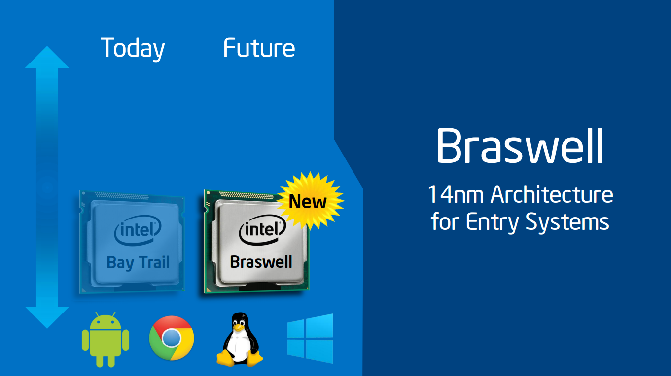
The Intel Celeron N3150 is a quad-core SoC for entry-level notebooks, which has been presented in early 2015. It is clocked at 1.6 - 2.08 GHz and part of the Braswell platform. Thanks to its new 14 nanometer low-power process (P1273) with tri-gate transistors, energy efficiency has been significantly improved compared to its predecessor Bay Trail (e.g. Celeron N2930). In addition to the CPU cores, the SoC offers a DirectX 11.2-capable GPU as well as a DDR3L Memory Controller (2x 64 bit, 25.6 GB/s).
Architecture
The processor cores are based on the Airmont architecture, which is basically a slightly modified shrink of the previous Silvermont core. While performance per clock has not been improved, the more efficient 14 nm process may lead to a better utilization of the CPU Burst (alias Turbo Boost) and therefore a somewhat higher performance in certain situations.
Performance
Compared to its predecessor Celeron N2930 (1.8 - 2.2 GHz) or the competing AMD APU E2-6110, the N3150 offers an almost identical performance. Using Windows, the CPU is adequate for everyday tasks such as Internet browsing or office applications, but may struggle in more demanding software.
Graphics
The HD Graphics (Braswell) is based on the Intel Gen8 architecture, which supports DirectX 11.2 and is also found in the Broadwell series (e.g. HD Graphics 5300). With 12 EUs (Execution Units) and a clock speed of up to 640 MHz, the GPU is almost twice as fast as the HD Graphics (Bay Trail), but still not powerful enough to handle demanding 3D games of 2015. The GPU also supports 4K/H.265 video acceleration.
Power Consumption
The entire SoC is rated at an TDP of 6 watts (SDP 4 watts). Thus, the chip can be cooled passively.
Intel Celeron N5105
► remove from comparisonThe Intel Celeron N5105 is a quad-core SoC of the Jasper Lake series that is primarily intended for inexpensive desktops and was announced in early 2021. The four Tremont CPU cores clock between 2 and 2.9 GHz (single core Burst) and offer no HyperThreading (SMT). The N5105 uses 1.5 MB L2 and 4 MB L3 cache. The chip is manufactured in 10nm at Intel (most likely in the same process as Ice Lake).
CPU Architecture
The processor architecture is called Tremont and a complete redesign compared to the old Golmont Plus cores in the predecessor. According to Intel, the single thread performance of a core could be improved by 30% on average (10 - 80% in all tests of SPECint and SPECfp).
Features
In addition to the quad-core CPU block, the SoC integrates a 24 EU Intel UHD Graphics GPU clocked from 450 - 800 MHz and a LPDDR4(x) dual channel memory controller (up to 16 GB and 2933 MHz). The chip now also partly integrates Wi-Fi 6 (Gig+), 8 PCIe 3.0 lanes, 14 USB 2.0/ 3.2 ports and two SATA 6.0 ports. The package got bigger and measures 35 x 24 mm (compared to 25 x 24 mm for the N5030 e.g.). The SoC is directly soldered to the mainboard (BGA) and can't be easily replaced.
Performance
The average N5105 in our database is in the same league as the Core i3-1005G1 and the Ryzen 3 3250U, as far as multi-thread benchmark scores are concerned. Your mileage may vary depending on how high the CPU power limits are.
Power Consumption
Similar to the predecessor, Intel specifies the TDP with 10 Watts (mobile and lower clocked N5100 6W). The chip can therefore be cooled passively in theory, but SKUs with fans are possible as well.
| Model | Intel Celeron N3150 | Intel Celeron N5105 | ||||||||||||||||||||||||||||||||||||||||||||||||||||
| Codename | Braswell | Jasper Lake | ||||||||||||||||||||||||||||||||||||||||||||||||||||
| Series | Intel Celeron | Intel Jasper Lake | ||||||||||||||||||||||||||||||||||||||||||||||||||||
| Series: Jasper Lake Jasper Lake |
|
| ||||||||||||||||||||||||||||||||||||||||||||||||||||
| Clock | 1600 - 2080 MHz | 2000 - 2900 MHz | ||||||||||||||||||||||||||||||||||||||||||||||||||||
| L2 Cache | 2 MB | 1.5 MB | ||||||||||||||||||||||||||||||||||||||||||||||||||||
| Cores / Threads | 4 / 4 | 4 / 4 | ||||||||||||||||||||||||||||||||||||||||||||||||||||
| TDP | 6 Watt | 10 Watt | ||||||||||||||||||||||||||||||||||||||||||||||||||||
| Technology | 14 nm | 10 nm | ||||||||||||||||||||||||||||||||||||||||||||||||||||
| max. Temp. | 90 °C | 105 °C | ||||||||||||||||||||||||||||||||||||||||||||||||||||
| Socket | FCBGA1170 | BGA1338 | ||||||||||||||||||||||||||||||||||||||||||||||||||||
| Features | Intel HD Graphics (Braswell, 12 EUs, 320 - 640 MHz), Wireless Display, Quick Sync, AES-NI, max. 8 GB Dual-Channel DDR3L-1600 (25,6 GB/s), 5x USB 3.0, 4x PCIe 2.0, 2x SATA 6.0 Gbit/s | DDR4-2933/LPDDR4x-2933 RAM, PCIe 3, GNA, MMX, SSE, SSE2, SSE3, SSSE3, SSE4.1, SSE4.2, VMX, SMEP, SMAP, EIST, TM1, TM2, Turbo, AES-NI, RDRAND, RDSEED, SHA | ||||||||||||||||||||||||||||||||||||||||||||||||||||
| iGPU | Intel HD Graphics (Braswell) (320 - 640 MHz) | Intel UHD Graphics (Jasper Lake 24 EU) (450 - 800 MHz) | ||||||||||||||||||||||||||||||||||||||||||||||||||||
| Architecture | x86 | x86 | ||||||||||||||||||||||||||||||||||||||||||||||||||||
| $107 U.S. | ||||||||||||||||||||||||||||||||||||||||||||||||||||||
| Announced | ||||||||||||||||||||||||||||||||||||||||||||||||||||||
| Manufacturer | ark.intel.com | ark.intel.com | ||||||||||||||||||||||||||||||||||||||||||||||||||||
| L3 Cache | 4 MB |

Benchmarks
Average Benchmarks Intel Celeron N3150 → 100% n=6
Average Benchmarks Intel Celeron N5105 → 336% n=6
* Smaller numbers mean a higher performance
1 This benchmark is not used for the average calculation