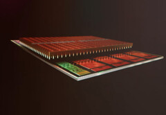
The jump to Zen 4 is not happening this year, but AMD already has an answer for Intel’s Alder Lake platform. As announced at Computex earlier this summer, AMD will upgrade its Zen 3 processors with the 3D V-Cache technology in early 2022, and this should be enough to even the playing field against Intel, at least until the next gen is launched in late 2022. At the Hot Chips annual symposium, AMD recently provided more details on how 3D V-Cache works and also offered a preview for its future 3D stacking applications.
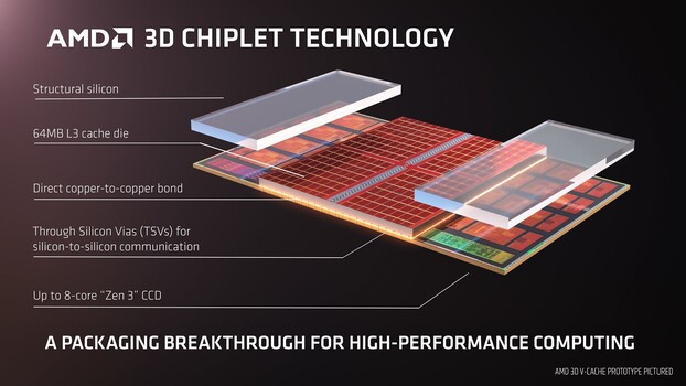
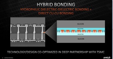
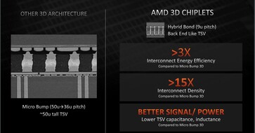
AMD is implementing a 9 micron Micro Bump 3D chiplet package for the V-Cache through silicon via (TSV). Although only 1 micron thinner than Intel’s Foveros 3D stacking that will be used to produce the Alder Lake processors, the Micro Bumps from AMD are said to offer more than 3 times the interconnect energy efficiency, 15 times interconnect density and capacitance/inductance. The current TSV technology that acts as a vertical inter-wafer or inter-die connection does not offer too many bonds, but, in the future, the TSV pitch will become more and more refined, allowing for more complex 3D stacking designs. V-Cache, for instance, allows for full silicon-to-silicon communication (DRAM on CPU / CPU on CPU) via direct copper-to-copper bonds. This enables the addition of 64 MB of L3 cache to the existing amount, which is supposed to provide a performance increase of 15% in games and 19% in content creation applications.
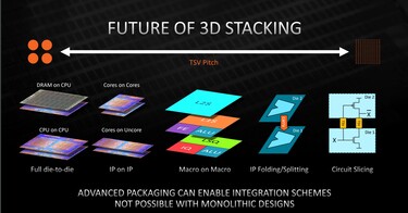
Finer TSV pitches will allow complex 3D stacking techniques including IP on IP ( cores on cores / cores on uncore), macro on macro (SoCs on SoCs), and eventually even IP folding / splitting and circuit slicing. Power requirements will also decrease by more than 3 times. We will probably see the first application of the IP on IP technique with the RDNA2 GPU cores stacked on top of the Zen 4 cores.


