OG Switch to get upgraded Nvidia Tegra X1 chip in mid-cycle revamp

While the new Nintendo Switch Lite is grabbing all the headlines, Nintendo has quietly sought FCC approval for what is called a "Class II Permission Change" as part of the certification process for a mid-cycle revamp of the original Switch hybrid console. The process allows for the certification of a device that has previously been certified after modifications have been applied to the design. The aim of the process is to save having to undergo a full recertification.
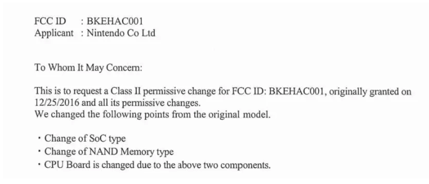
For gadget lovers, the process has yielded the specific details of the design changes that Nintendo is making. These include a change of SoC, NAND memory type and a CPU board change to accommodate the new components. We already know that the Switch features an ageing Tegra X1 chip that has an ARM-based design dating back to 2015 and fabricated on a similarly ageing 20nm node. Nintendo has confirmed that the Switch Lite features an updated version of this chip, although it hasn't detailed exactly what the changes are; however, we can make an educated guess.
Given the Switch Lite is said to be more power efficient the OG Switch, it makes sense to think that Nvidia has switched to a newer fabrication node, perhaps at least 14nm or even 10nm. With the Switch Lite capable of playing all compatible Switch games (i.e those without the need for Joy-Con support), it would also make sense for Nintendo to put the same upgraded internals in a mid-cycle upgrade of the Switch. While performance may or may not get a boost, at the very least, it will offer better battery life if not also faster loading times thanks to the new NAND memory.