Rumour | Detailed evidence of AMD's first post-Navi GPU appears online sporting 32 GB of HBM2 memory
TechPowerUp reports that it is received the BIOS of AMD's first post-Navi GPU, a card that may feature up to 1 TB/s memory bandwidth. It is not an example of the "Big Navi" to which AMD alluded at CES 2020, though. On the contrary, TechPowerUp claims that it is essentially a stripped-back Vega chip.
The new leak follows yesterday's, on which we also reported. On the face of things, it appears that these two leaks come from different sources. While yesterday's evidently came from @KOMACHI_ENSAKA, TechPowerUp cites an unnamed source. @KOMACHI_ENSAKA has since explained that it had cooperated with the website, presumably supplying it with the BIOS. However, it had requested that TechPowerUp wait until the announcement of the GPU before publishing details pulled from the BIOS, a request that the website ignored.
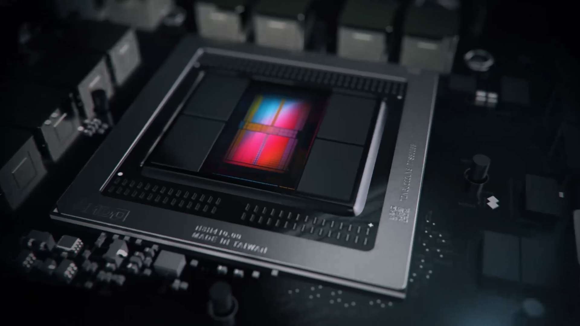
Apparently called the Radeon Instinct MI100, the sever accelerator is the first example of AMD's Arcturus architecture. According to TechPowerUp, the card carries the device ID "0x1002 0x738C", which it states confirms that it is an AMD Arcturus chip. The website also reports that the card has 32 GB of HBM2 memory, along with support for Samsung KHA884901X and Hynix H5VR64ESA8H. Combining this with a 1,000 MHz clock speed and a 4,096-bit bus may yield a 1 TB/s memory bandwidth too.
TechPowerUp has also deduced from the BIOS that the GPU has a 1,334 MHz clock speed, with the SoC running at 1,091 MHz. Meanwhile, the 128 Compute Unit (CU) and 8,192 shader unit part reports a 200 W thermal design power (TDP), a value that is far lower than recent high-end AMD GPUs. TechPowerUp speculates that this could either mean that the MI100 is more efficient than past AMD cards, or that it is currently reporting an incorrect TDP.
Moreover, the MI100 is effectively a Vega card with the 3D graphics capabilities removed. Hence, it is not the first sighting of a "Big Navi" GPU, which could well be a series of Navi 20 cards that will succeed the RX 5700 series later this year. Instead, expect AMD to launch this Arcturus GPU as a new Instinct card in the near future.
Source(s)
Freedesktop.org (1) (2) & @KOMACHI_ENSAKA via TechPowerUp & Videocardz