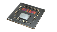
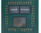
We have previously reported on AMD patents pertaining to a hybrid CPU architecture similar to Intel's upcoming Alder Lake family and ARM's big.LITTLE processor clusters. Now, we are getting to know that this hybrid approach may soon be a reality with Zen 5 Ryzen 8000 expected to launch some time in 2024.
According to a report by Moepc shared by @Avery78 on Twitter, AMD Zen 5 apparently codenamed Strix Point will feature a big,LITTLE-esque architecture with eight large Zen 5 cores made on TSMC's 3 nm process and four small cores of which details aren't yet available.
We know that AMD will be including iGPUs even for mainstream processors from Ryzen 7000 Raphael onwards. In fact, Raphael is expected to sport a Navi 21 iGPU. Moepc states that AMD has already fixed the iGPU performance target for Zen 5 Strix Point, but the publication hasn't divulged any further detail apart from stating that the memory subsystem will sport "bigger changes".
The above information should be taken with a healthy dose of skepticism considering that we are still a few years away from Zen 5's launch. We also do not know what is the exact hybridization that AMD is looking at here and whether both the big and small cores are Zen 5 or will be a mix of Zen 4 and Zen 5 for better utilization.
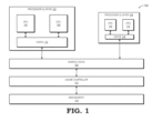
From what we know via available patent diagrams, both the big and small CPU clusters could have their own independent L1 caches, but we are still not sure how they would interface with subsequent cache levels. One of the three probable methods described in the patent suggests shadow-writing the thread state of small cluster L1 to big cluster L1, so that the bigger cores can immediately start executing threads passed on from the smaller ones.
Moepc reports that TSMC is currently on schedule for testing 3 nm in 2021 to be followed by high volume manufacturing in H2 2022. Apple is said to be another big customer for TSMC's 3 nm node apart from AMD. It is too early to speculate the kind of performance and efficiency gains that can be expected, but TSMC had previously indicated that the 3 nm node allows for up to 25 to 30% reduced power consumption, 10 to 15% increased performance, and a 1.7x increased transistor density compared to the 5 nm process.
Source(s)
Moepc via @Avery78 on Twitter and Videocardz


