

Apple A13 Bionic vs Qualcomm Snapdragon 855+ / 855 Plus vs Apple A12 Bionic
Apple A13 Bionic
► remove from comparison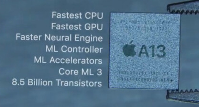
The Apple A13 Bionic is a System on a Chip (SoC) from Apple that is found in the iPhone 11 series. It was announced late 2019 and offers 6 cores divided in 2 performance cores and four power efficiency cores. Compared to the previous A12 Bionic, the A13 should offer a 20% improved CPU performance at 40% lower power (according to Apple).
With 8.5 billion transistors, the A13 Bionic is a big chip especially compared to the Snapdragon 835 (3 Billion) or a Skylake desktop quad-core Soc (1.75 Billion).
Qualcomm Snapdragon 855+ / 855 Plus
► remove from comparisonThe Qualcomm Snapdragon 855 Plus (855+) Mobile Platform is a high-end smartphone and tablet SoC that Qualcomm announced in 2019. Compared to the normal Snapdragon 855, the 855 Plus offers higher clock speeds of the GPU and CPU. The SoC integrates a fast ‘Prime Core’ that clocks up to 2.96 GHz (up from 2.84 GHz in the 855) and three further fast ARM Cortex-A76 performance cores, which can reach up to 2.42 GHz. These are complemented by four power-saving ARM Cortex-A55 cores that clock up to a maximum of 1.8 GHz.
The SoC also integrates the new X24 LTE modem that Qualcomm promises will deliver up to 2 Gbit/s maximum download speed over LTE Cat.20 and up to 316 Mbit/s upload speeds. The Snapdragon 855 can be configured with the company’s new X50 5G modem too.
Qualcomm has also improved the integrated Wi-Fi modem, which is Wi-Fi 6-ready, has 8x8 Sounding and supports up to 802.11 ay Wi-Fi. The Wi-Fi modem can utilise the 60 GHz mmWave band for up to 10 Gbit/s internet speeds.
The Hexagon 690 DSP has undergone the most revisions of that which Qualcomm has integrated into the Snapdragon 855. The new DSP incorporates a neural processing unit (NPU) with dedicated Tensor-cores that can execute up to 7 trillion operations per second in conjunction with the CPU and GPU. In short, the Snapdragon 855 should be three times faster than the Snapdragon 845 and two times faster than the Kirin 980 SoC.
The Snapdragon 855 also has a Spectra 380 ISP onboard, which is the world’s first chip to incorporate a Computer Vision Engine (CV-ISP) that can perform depth calculations in videos at up to 60 FPS. The Snapdragon 855 should deliver real-time portrait modes or be able to detect objects with relatively low power consumption.
The built-in memory controller supports up to 16 GB LPDDR4x RAM (4 x 16-bit). As the SD855, the 855+ integrates an Adreno 640 graphics card that is now higher clocked and should offer a 15% higher performance.
Qualcomm will manufacturer the Snapdragon 855+ at the Taiwan Semiconductor Manufacturing Company (TSMC) using a 7 nm FinFET process.
Apple A12 Bionic
► remove from comparison
The Apple A12 Bionic is a System on a Chip (SoC) from Apple that is found in the iPhone Xs and Xr. It was announced late 2018 and offers 6 cores divided in 2 performance cores and four power efficiency cores. Compared to the previous A11 Bionic, the A12 should offer a 15% improved CPU performance for the performance cores and a 50% lower power consumption for the efficiency cores (both according to Apple).
The chip also includes a new GPU that is advertised as 50% faster, the M12 Motion co-processor and a Neural Engine with 8 cores for up to 5 trillion operations per second.
With 6.9 billion transistors, the A12 Bionic is a big chip especially compared to the Snapdragon 835 (3 Billion) or a Skylake desktop quad-core Soc (1.75 Billion). Compared to the A11, the A12 integrates 60% more transistors.
| Model | Apple A13 Bionic | Qualcomm Snapdragon 855+ / 855 Plus | Apple A12 Bionic | ||||||||||||||||||||||||||||||||||||||||||||
| Codename | Lightning and Thunder | Cortex-A76 / A55 (Kryo 485) | |||||||||||||||||||||||||||||||||||||||||||||
| Series | Apple Apple A-Series | Qualcomm Snapdragon | Apple Apple A-Series | ||||||||||||||||||||||||||||||||||||||||||||
| Clock | <=2660 MHz | <=2960 MHz | <=2490 MHz | ||||||||||||||||||||||||||||||||||||||||||||
| L1 Cache | 832 KB | 256 KB | |||||||||||||||||||||||||||||||||||||||||||||
| L2 Cache | 12 MB | 1.8 MB | 8 MB | ||||||||||||||||||||||||||||||||||||||||||||
| Cores / Threads | 6 / 6 | 8 / 8 | 6 / 6 | ||||||||||||||||||||||||||||||||||||||||||||
| Transistors | 6900 Million | 6900 Million | |||||||||||||||||||||||||||||||||||||||||||||
| Technology | 7 nm | 7 nm | 7 nm | ||||||||||||||||||||||||||||||||||||||||||||
| Features | ARMv8 Instruction Set | X24 LTE Modem, Adreno 640 GPU | ARMv8 Instruction Set | ||||||||||||||||||||||||||||||||||||||||||||
| iGPU | Apple A13 Bionic GPU | Qualcomm Adreno 640 (250 - 675 MHz) | Apple A12 Bionic GPU | ||||||||||||||||||||||||||||||||||||||||||||
| NPU / AI | 6 TOPS INT8 | 5 TOPS INT8 | |||||||||||||||||||||||||||||||||||||||||||||
| Architecture | ARM | ARM | ARM | ||||||||||||||||||||||||||||||||||||||||||||
| Announced | |||||||||||||||||||||||||||||||||||||||||||||||
| Series: Apple A-Series |
|
| |||||||||||||||||||||||||||||||||||||||||||||
| L3 Cache | 5 MB | ||||||||||||||||||||||||||||||||||||||||||||||
| TDP | 5 Watt | ||||||||||||||||||||||||||||||||||||||||||||||
| Manufacturer | www.qualcomm.com |

Benchmarks
Average Benchmarks Apple A13 Bionic → 100% n=21
Average Benchmarks Qualcomm Snapdragon 855+ / 855 Plus → 83% n=21
Average Benchmarks Apple A12 Bionic → 83% n=21
* Smaller numbers mean a higher performance
1 This benchmark is not used for the average calculation