A look inside an Anker GaN charger
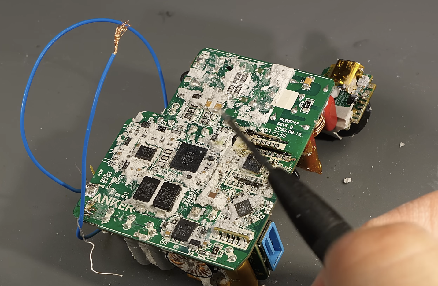
YouTuber Zerobrain is currently providing a highly interesting look inside a defective Anker charger. The charger is a typical GaN device with USB Power Delivery on two USB-C ports and one USB-A port. GaN chargers are known for being particularly compact but also for generating a fair amount of heat. Zerobrain originally wanted to take the charger apart to find out why it had failed. In the process, he provides a detailed look at its internals and therefore at the charger's construction. This is something that is normally not visible and should not be attempted, since even a switched-off charger can still carry dangerous residual voltage.
Zerobrain cannot determine the actual fault in the video with 100% certainty, but the process itself provides plenty of information and images showing how a modern charger like this is built. These devices are packed to the brim. As Zerobrain acknowledges, Anker did its homework and created a safe design. Repairs are difficult, however, because the internals are heavily glued in place. This helps prevent problems caused by vibration. After all, mains voltage must not come into contact with USB voltage just because something moves and comes loose.
Over the course of the roughly 20-minute video, he also manages to expose most of the charger's circuit board. The charger itself is an older design. The circuit board dates from September 2023, though some additional time has to be factored in between a board's development, its installation in a charger and the product actually reaching the market. Even though he does not find the exact reason for the failure, seeing just how densely a modern charger is built is interesting in any case.
Source(s)
Youtube
No comments for this article

