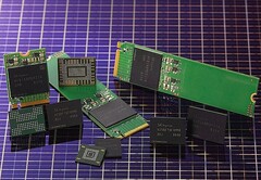
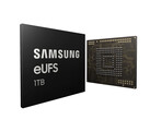
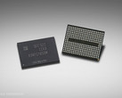
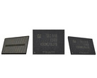
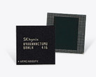
SK Hynix is back with a new NAND Flash chip that will enter the mass production stage before the end of the year. The new chip is the world's first 96-layer 512 Gb 4D NAND Flash, and it involves quite a few technologies: a 3D CTF (Charge Trap Flash) design paired with PUC (Peri Under Cell), as well as rather traditional TLC (Triple-Level Cell) arrays.
The chip is the industry's first one that brings together 3D CTF and PUC, SK Hynix naming this product "CTF-based 4D NAND Flash" to separate it from the existing 3D NAND Flash solutions. In terms of performance, Hynix unveiled the following details:
- industry-leading 64 KB bandwidth
- I/O speed up to 1,200 Mbps at 1.2 V
- 30 percent higher write and 25 read performance compared to the 72-layer 512 Gb 3D NAND
- 30 percent smaller chip size and 49 percent bit productivity per wafer increase vs. the 72-layer 512 Gb 3D NAND
In the future, the company expects to introduce 1 TB SSDs with Hynix controllers and UFS 3.0 solutions, as well as 96-layer 1 Tb TLC and QLC (Quad-Level Cell) chips. All these should arrive in 2019.


