 Deutsch
 English
 Español
 Français
 Italiano
 Nederlands
 Polski
 Português
 Русский
 Türkçe
 Svenska
 Chinese
 Magyar
AMD Ryzen 9 6980HS vs AMD Ryzen 9 PRO 6950HS
AMD Ryzen 9 6980HS
► remove from comparison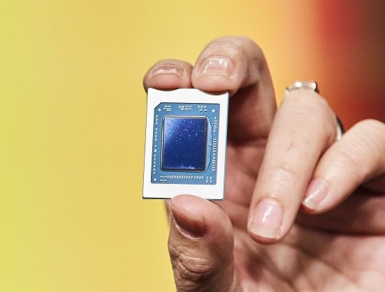
The AMD Ryzen 9 6980HS is a processor for big (gaming) laptops based on the Rembrandt generation. R9 6980HS integrates all eight cores based on the Zen 3+ microarchitecture. They are clocked at 3.3 (guaranteed base clock) to 5 GHz (Turbo) and support SMT / Hyperthreading (16 threads). The chip is manufactured on the modern 6 nm TSMC process.
The new Zen 3+ is a refresh of the Zen 3 architecture and should not offer a lot of changes. The chip itself however, offers a lot of new features, like support for USB 4 (40 Gbps), PCI-E Gen 4, DDR5-4800MT/s or LPDDR5-6400MT/s, WiFi 6E, Bluetooth LE 5.2, DisplayPort 2, and AV1 decode.
A big novelty is the integrated GPU Radeon 680M, that is now based on the RDNA2 architecture and offers 12 CUs at up to 2.4 GHz. It should be the fastest iGPU of all at the time of announcement.
Performance
While we have not tested a single system powered by the 6980HS as of August 2023, it's safe to expect the chip to be about as fast as the 6950HS, 6950H, 6980HX.
Your mileage may vary depending on how high the CPU power limits are, and how competent the cooling solution of your system is.
Power Consumption
This Ryzen 9 has a default TDP of 35 W (also known as the PL1). Which is definitely too high to allow for passively cooled designs.
The APU is built with TSMC's 6 nm process for great, as of late 2022, energy efficiency.
AMD Ryzen 9 PRO 6950HS
► remove from comparisonThe AMD Ryzen 9 PRO 6950HS is a processor for big (workstation) laptops based on the Rembrandt generation. The R9 6950HS integrates all eight cores based on the Zen 3+ microarchitecture. They are clocked at 3.3 (guaranteed base clock) to 4.9 GHz (Turbo) and support SMT / Hyperthreading (16 threads). The chip is manufactured on the modern 6 nm TSMC process. The HS variant offers a 10 W lower TDP and therefore a lower sustained performance than the HX version. Professional version of the consumer R7 6800HS with additional managment features and the Microsoft Pluton Security processor.
The new Zen 3+ is a refresh of the Zen 3 architecture and should not offer a lot of changes. The chip itself however, offers a lot of new features, like support for USB 4 (40 Gbps), PCI-E Gen 4, DDR5-4800MT/s or LPDDR5-6400MT/s, WiFi 6E, Bluetooth LE 5.2, DisplayPort 2, and AV1 decode.
A big novelty is the integrated GPU Radeon 680M, that is now based on the RDNA2 architecture and offers 12 CUs at up to 2.4 GHz. It should be the fastest iGPU of all at the time of announcement.
Performance
The average 6950HS in our database is in the same league as the Intel Core i7-1280P, AMD Ryzen 9 4900H, Intel Core i7-11800H, as far as multi-thread benchmark scores are concerned - which puts it somewhat behind the mighty 12th Gen Alder Lake-H processors. This Ryzen 9 series chip is still more than good enough for proper gaming on the go as well as content creation, as of mid 2022.
Your mileage may vary depending on how high the CPU power limits are and how competent the cooling solution of your system is.
Power consumption
The Ryzen has a default TDP of 35 W (also known as PL1). That's too high to allow for a passively cooled design.
The APU is built with TSMC's 6 nm process for great, as of late 2022, energy efficiency.
| Model | AMD Ryzen 9 6980HS | AMD Ryzen 9 PRO 6950HS | ||||||||||||||||||||||||||||||||||||||||||||||||
| Series | AMD Rembrandt (Zen 3+) | AMD Rembrandt (Zen 3+) | ||||||||||||||||||||||||||||||||||||||||||||||||
| Codename | Rembrandt-HS (Zen 3+) | Rembrandt-HS (Zen 3+) | ||||||||||||||||||||||||||||||||||||||||||||||||
| Series: Rembrandt (Zen 3+) Rembrandt-HS (Zen 3+) |
|
| ||||||||||||||||||||||||||||||||||||||||||||||||
| Clock | 3300 - 5000 MHz | 3300 - 4900 MHz | ||||||||||||||||||||||||||||||||||||||||||||||||
| L1 Cache | 512 KB | 512 KB | ||||||||||||||||||||||||||||||||||||||||||||||||
| L2 Cache | 4 MB | 4 MB | ||||||||||||||||||||||||||||||||||||||||||||||||
| L3 Cache | 16 MB | 16 MB | ||||||||||||||||||||||||||||||||||||||||||||||||
| Cores / Threads | 8 / 16 | 8 / 16 | ||||||||||||||||||||||||||||||||||||||||||||||||
| TDP | 35 Watt | 35 Watt | ||||||||||||||||||||||||||||||||||||||||||||||||
| Technology | 6 nm | 6 nm | ||||||||||||||||||||||||||||||||||||||||||||||||
| max. Temp. | 95 °C | 95 °C | ||||||||||||||||||||||||||||||||||||||||||||||||
| Socket | FP7/FP7r2 | FP7/FP7r2 | ||||||||||||||||||||||||||||||||||||||||||||||||
| Features | DDR5-4800/LPDDR5-6400 RAM (incl. ECC), PCIe 4, MMX, SSE, SSE2, SSE3, SSSE3, SSE4A, SSE4.1, SSE4.2, AVX, AVX2, BMI2, ABM, FMA, ADX, SMEP, SMAP, SMT, CPB, AES-NI, RDRAND, RDSEED, SHA, SME | DDR5-4800/LPDDR5-6400 RAM (incl. ECC), PCIe 4, PRO, MMX, SSE, SSE2, SSE3, SSSE3, SSE4A, SSE4.1, SSE4.2, AVX, AVX2, BMI2, ABM, FMA, ADX, SMEP, SMAP, SMT, CPB, AES-NI, RDRAND, RDSEED, SHA, SME | ||||||||||||||||||||||||||||||||||||||||||||||||
| iGPU | AMD Radeon 680M ( - 2400 MHz) | AMD Radeon 680M ( - 2400 MHz) | ||||||||||||||||||||||||||||||||||||||||||||||||
| Architecture | x86 | x86 | ||||||||||||||||||||||||||||||||||||||||||||||||
| Announced | ||||||||||||||||||||||||||||||||||||||||||||||||||
| Manufacturer | www.amd.com | www.amd.com |
