




Kirin 9030 Pro teardown reveals China's new playbook for advanced chipmaking
The Kirin 9030 Pro powers Huawei's newest Mate 80 Pro and Mate 80 Pro Max. It is manufactured by China's largest foundry, SMIC, on its cutting-edge N+3 node. SemiAnalysis got a chance to tear it apart and look at what makes it tick, and found some surprising results. The Kirin 9030 Pro features a minimum (M0) metal pitch of just 32.5 nm, slightly tighter than the 36 nm found on Intel's Panther Lake processors built on its 18A process.
The finding appears remarkable because Intel manufactures its latest chips using extreme ultraviolet (EUV) lithography, while SMIC remains locked out of ASML's EUV scanners due to years of U.S.-led export restrictions, relying instead on older deep ultraviolet (DUV) equipment. The teardown gives us insights into how far Chinese chipmakers have pushed mature manufacturing technologies through increasingly clever engineering, while also highlighting the limits of judging semiconductor processes by a single metric.
What exactly is metal pitch?
The chip's minimum metal pitch is often referred to as the M0 layer. Modern processors contain numerous layers of microscopic copper wiring that connect billions of transistors together. Metal pitch simply describes the distance separating adjacent wires. The smaller that spacing becomes, the more routing resources (and consequently more logic) can fit inside the same area.
SemiAnalysis measured the Kirin 9030 Pro's smallest routing layer at 32.5 nm, compared with approximately 40 nm on MediaTek's Helio G99 manufactured on TSMC's N6 process. The publication estimates SMIC's N+3 process reaches roughly 113 million transistors per square mm, marginally exceeding TSMC N6's estimated density of 108 million transistors per square mm. Those figures are impressive considering SMIC's process relies exclusively on DUV lithography while Intel and TSMC use EUV on 18A and N6, respectively.
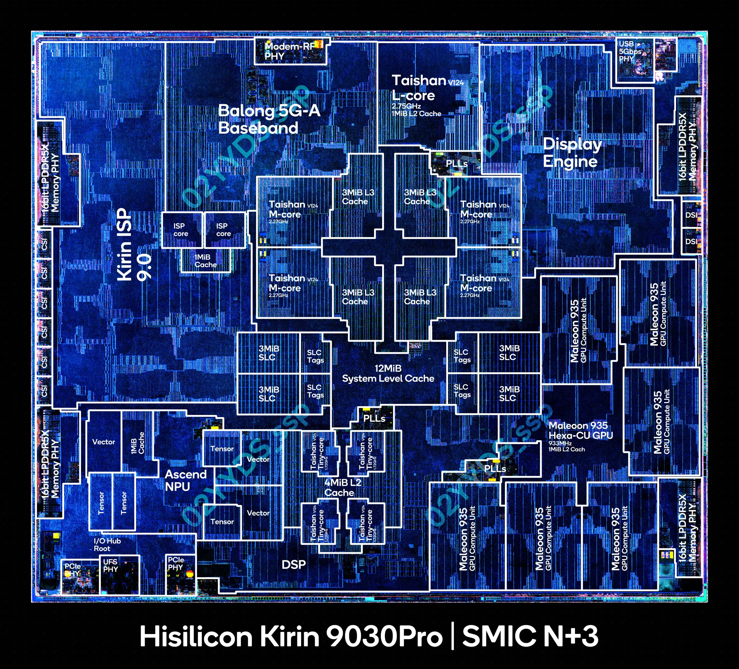
We also get a detailed die shot from X user @HiEq_2005 that highlights the Kirin 9030’s key components, such as Huawei's custom Taishan V124 CPU cores, paired with a Maleoon 935 GPU, an Ascend NPU, an integrated Balong 5G-A modem, dedicated image signal processors, display engine, DSP and an expansive cache hierarchy, including a 12 MB System Level Cache (SLC) surrounded by multiple distributed L3 cache slices.
How SMIC pushed DUV further than expected
The pressing question is how SMIC managed to achieve EUV-class density without EUV. The answer lies in manufacturing complexity. Rather than printing extremely fine circuit features directly, SMIC relies heavily on Self-Aligned Quadruple Patterning (SAQP), an advanced lithography technique that effectively multiplies the resolution of older DUV equipment.
The process begins by printing a relatively coarse pattern before depositing thin spacer materials along its edges. Those spacers then become a new mask capable of defining even narrower structures. Repeating the procedure multiple times allows engineers to create features far smaller than the original exposure would normally permit.
Every additional lithography pass requires another mask, another alignment stage and another opportunity for manufacturing defects. More process steps translate directly into higher wafer costs, lower yields and longer production times. SMIC is effectively compensating for the lack of EUV through manufacturing persistence rather than fundamentally superior lithography.
Density isn't achieved through lithography alone
Lithographic ingenuity aside, SemiAnalysis attributes much of SMIC's density gains to Design Technology Co-Optimization (DTCO), a methodology that develops semiconductor manufacturing and chip architecture together instead of treating them as independent disciplines.
Rather than relying exclusively on smaller transistors, engineers optimise standard logic cells themselves, shrinking isolation regions, relocating contacts, reducing transistor fins and reorganising layouts to extract incremental space savings.
Instead of dedicating the majority of its die area to CPU cores, Huawei dedicates a good chunk of it to cache. Large caches reduce expensive trips to external LPDDR5X memory, improving latency while simultaneously lowering power consumption.
Semiconductor performance depends as much on intelligent data movement as it does on transistor scaling, and the Kirin 9030 Pro is a testament to how architectural optimisation has become just as important as manufacturing technology itself.
Performance tells a different story
The Kirin 9030 Pro's, and by extension SMIC’s, shortcomings become apparent when examining real-world performance. Huawei's latest flagship CPU performs roughly on par with premium Android processors from several years ago despite its competitive transistor density. The efficiency gap is even larger.
SemiAnalysis notes Apple's small efficiency cores can outperform Huawei's prime CPU core in certain integer workloads while consuming roughly one watt of power, compared with approximately 4.5 watts for Huawei's highest-performance core. Likewise, the Taishan architecture delivers performance comparable to Arm's Cortex-X2 from 2021, while Apple's M1 processor from 2020 still achieves substantially higher instructions-per-clock at similar power levels.
The Kirin 9030 Pro therefore demonstrates an important reality of modern semiconductor development: transistor density alone no longer defines leadership.
China's semiconductor industry has lofty aims
The teardown ultimately tells a much broader story than one impressive measurement under an electron microscope. Export controls have unquestionably slowed China's semiconductor ambitions, but they have also forced companies like Huawei and SMIC to pursue alternative paths. Rather than relying exclusively on traditional node shrinks, both companies appear increasingly focused on architectural optimisation.
Earlier this year, Huawei's He Tingbo introduced what the company calls the Tau Scaling Law at the IEEE International Symposium on Circuits and Systems (ISCAS). The framework proposes reducing signal propagation delay throughout a chip as the next major driver of semiconductor progress. Simply shrinking transistors is only one part of the puzzle.
Technologies such as LogicFolding, which reorganises circuit layouts to shorten critical wiring paths, sit at the heart of that strategy. Huawei says future Kirin processors launching later this year (likely the Kirin 9040) will be the first commercial chips to implement LogicFolding. The company believes its long-term roadmap could eventually achieve transistor densities comparable to 14 Angstrom (1.4 nm)-class manufacturing technologies by around 2031.
China may not remain dependent on DUV forever
According to a recent Reuters investigation, Chinese researchers have already constructed an operational prototype EUV lithography machine after years of reverse engineering Western technology. The prototype reportedly began testing in early 2025 and is capable of generating EUV light, although it has yet to manufacture functional chips and still trails ASML in critical areas such as precision optics. Sources cited by Reuters say the Chinese government hopes to produce chips using the system by around 2028, but 2030 is believed to be a more realistic target. If Huawei's architectural innovations eventually converge with domestically developed EUV lithography, China's semiconductor roadmap could look very different by the end of the decade.
Source(s)
 Add as a preferred source on Google


