Japanese foundry Rapidus is making cutting edge 2 nm nodes with IBM, plans to compete with TSMC and Samsung by 2027
Japan used to be the foundry hub of the world prior to Y2K, with over 50% of the semiconductor production recorded in 1988. Throughout the ‘90s, Japan slowly started losing ground to US, South Korean and Taiwanese-based foundries. By 2022, Japan’s semiconductor share had shrunk to 9% of the global market, even though the country still hosts the largest number of chip factories in the world. Two years ago, the Japanese government came up with a plan to restore the country’s former semiconductor glory by investing up to US$54 billion in a new foundry called Rapidus. Techspot reports that the project is highly ambitious, as Japan is now collaborating with IBM in order to catch up to TSMC or Samsung and provide cutting edge 2 nm production nodes by 2027.
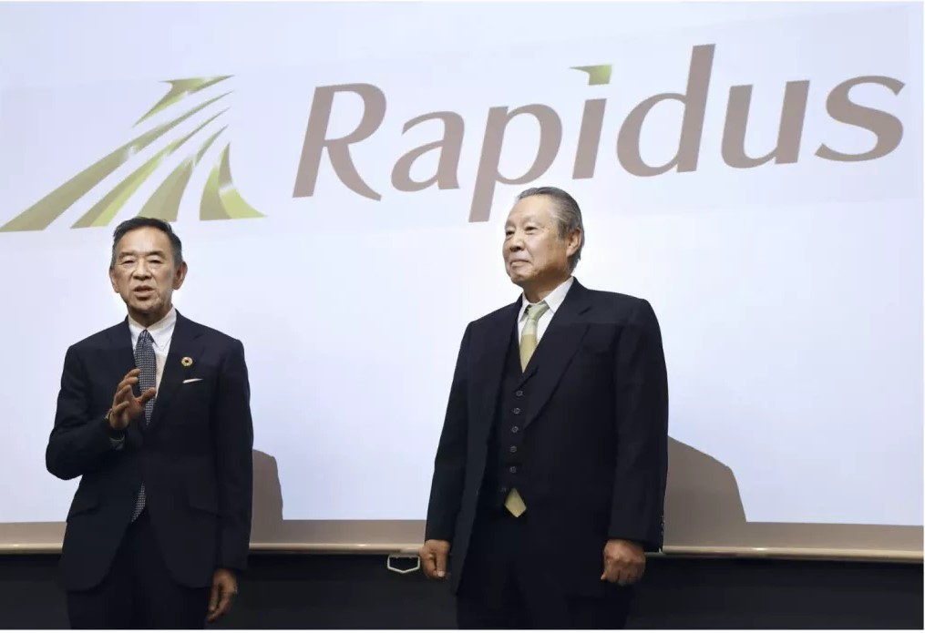
Rapidus was founded in 2022 by industry veteran Tetsuro Higashi, former president of Tokyo Electron, along with Atsuyoshi Koike, former president of Western Digital’s Japanese branch. Besides being heavily subsidized by the local authorities, Rapidus is backed by industry leading companies like Kioxia (Toshiba’s memory subsidiary), Sony, Toyota Motor, NEC and NTT plus financial giants such as Mitsubishi UFJ bank and SoftBank. IBM’s 2 nm designs presented in 2021 will serve as the basis for the cutting edge nodes planned by Rapidus. To this end, Rapidus is training all of its engineers at IBM’s research center in Albany, New York.
The Techspot report mentions that the 2 nm Rapidus production factory is set to be built in Chitose on the Hokkaido island of Japan. TSMC is also planning to build a facility for a Sony collaboration in this area. While the financial part appears to be covered by government subsidies and investments from powerful backers, Rapidus may still face significant challenges with the acquisition of the EUV lithography equipment from Dutch firm ASML. All the important foundries are fighting over these essential machines, and Rapidus could be looking at a 2-year lead time before securing any ASML lithography systems.
Chairman Tetsuro Higashi will not focus on direct competition with TSMC and Samsung from a production volume perspective. Instead, Rapidus will direct all efforts towards developing the most efficient 2 nm production nodes and eventually releasing angstrom-era technology before the big foundries.
Buy the Kioxia 1 TB SSD compatible with Dell, HP, Lenovo laptops on Amazon
Source(s)
