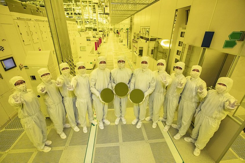
Samsung Foundry's 2 nm chips slated to enter mass production in 2025
Earlier last year, Samsung confirmed its flagship mobile AP for 2025, the Exynos 2500, would be manufactured on Samsung Foundry's 3GAP node. It is the second iteration of the often-forgotten 3GAA node that was relegated to manufacturing cryptocurrency mining ASICs. A new report from Business Korea says the company is on track to start mass production of its 2 nm node (SF2) next year.
Samsung Foundy will reveal more details about SF 2 at VLSI (Very Large Scale Integration) Symposium later this year. It will be used to develop Arm's upcoming Cortex-X6 CPU core. Even Qualcomm could eye up some capacity for its Snapdragon 8 Gen 5 for Galaxy SoC. Of course, Samsung will certainly use it for its own Exynos products, and AI chips from Japanese firm PFN.
It'll be interesting to see how it holds up against TSMC's 2 nm and Intel's 18A nodes, both of which are slated to enter mass production at around the same time. The competition will be tight this time around, as both Intel (RibbonFET) and TSMC (Nanosheets) have their own versions of gate-all-around transistors, something Samsung achieved with MBCFET in 2022.
Plus, SF2 could be the first Samsung Foundry node to introduce backside power delivery, which will also feature in Intel 18A (PowerVia) and TSMC N2P. For more information about how backside power delivery works, check out this excellent explainer by High Yield on YouTube.
Source(s)
