

Intel Celeron J1900 vs Intel Core i3-N300 vs Intel Celeron J1800
Intel Celeron J1900
► remove from comparison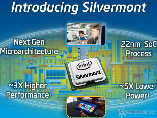
The Intel Celeron J1900 is a power efficient quad-core SoC for desktops and nettops. It is clocked at 2.0 - 2.42 GHz (Burst) and part of the Bay Trail-D platform. Thanks to the specially optimized 22 nanometer low-power process (P1271) with tri-gate transistors, performance and energy efficiency have been significantly improved compared to its predecessor.
Architecture
The processor cores are based on the new Silvermont architecture, which is an out-of-order design for the first time. The increased utilization of the pipeline and many other improvements (optimized branch prediction, increased buffers, enhanced decoders) have increased the performance per clock by about 50 percent. At the same time, however, the Hyper-Threading feature of the previous generation has been removed. Other major changes are the support for new instruction set extensions such as SSE 4.1 and 4.2 as well as AES-NI (depending on the model).
Performance
Thanks to 4 CPU cores and a clock speed of up to 2.42 GHz, the Celeron J1900 is significantly faster than previous Intel Atoms, e.g. the D2560. Presumably, the J1900 even outperforms the AMD Kabini APU A4-5000. For everyday tasks such as Internet or Office the performance is adequate, but not for very complex software or modern games.
Graphics
The HD Graphics (Bay Trail) is based on the Intel Gen7 architecture, which supports DirectX 11 and is also found in the Ivy Bridge series (e.g. HD Graphics 4000). With only 4 EUs (Execution Units) and a relatively low clock speed of up 688 - 854 MHz, the GPU is even slower than the HD Graphics (Ivy Bridge). Therefore, only older and less demanding games will run fluently.
Power Consumption
The entire SoC is rated at a TDP of 10 watts. Thus, the chip can be used in compact nettops.
Intel Core i3-N300
► remove from comparison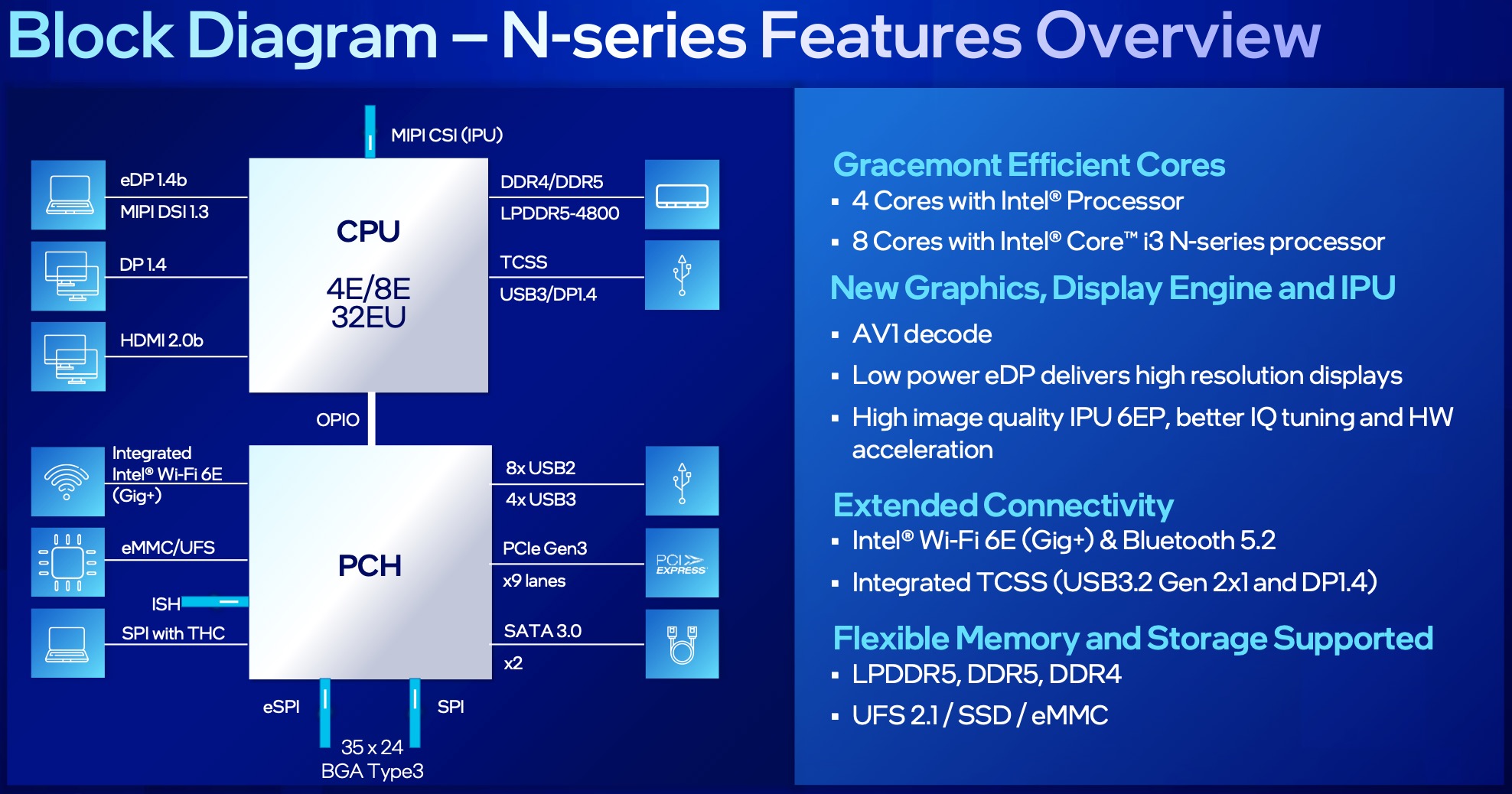
The Intel Core i3-N305 is an entry-level mobile CPU for thin and light laptops from the Alder Lake-N series. It was announced in early 2023 and offers no performance cores and 8 efficient cores (E-cores, Gracemont architecture). The chip does not support HyperThreading and clocks with up to 3.8 GHz (single core, 3 GHz all core Turbo). The performance of the E-cores should be similar to old Skylake cores (compare to the Core i7-6700HQ). All cores can use up to 6 MB L3-cache.
Performance
The performance depends on the cooling and TDP settings and should be somewhere similar to the old Alder Lake Pentium 8500 (1 performance core, 4 efficiency cores, max. 4.4 GHz and 8 MB L3-cache). The multi-threaded performance should be quite good with the 8 cores but will suffer due to the low TDP. Single thread performance will suffer due to the missing P-cores and relatively low boost clock speeds.
Features
The Alder Lake-N chips only support single channel memory with up to DDR5-4800, DDR4-3200 or LPDDR5-4800. The chip also supports Quick Sync and AV1 decoding (most likely same engine as in Alder Lake). Furthermore, Wi-Fi 6E and Bluetooth 5.2 are partly integrated (but no Thunderbolt). External chips can be connected via PCIe Gen3 x9 (via the PCH).
The integrated graphics adapter is based on the Xe-architecture and offersall 32 EUs (Execution Units) operating at up to 1.25 GHz. In addition to the single channel memory, the gaming performance is very limited of the iGPU.
Power consumption
The i3 has a base power consumption of 7 W and is therefore even suited for fanless cooling. The CPU is built with a further improved 10nm SuperFin process at Intel (called Intel 7).
Intel Celeron J1800
► remove from comparison
The Intel Celeron J1800 is a power efficient dual-core SoC for desktops and nettops. It is clocked at 2.41 - 2.58 GHz and part of the Bay Trail-D platform. Thanks to the specially optimized 22 nanometer low-power process (P1271) with tri-gate transistors, performance and energy efficiency have been significantly improved compared to its predecessor.
Architecture
The processor cores are based on the new Silvermont architecture, which is an out-of-order design for the first time. The increased utilization of the pipeline and many other improvements (optimized branch prediction, increased buffers, enhanced decoders) have increased the performance per clock by about 50 percent. At the same time, however, the Hyper-Threading feature of the previous generation has been removed. Other major changes are the support for new instruction set extensions such as SSE 4.1 and 4.2 as well as AES-NI (depending on the model).
Performance
Thanks to the improved performance per clock, the Celeron J1800 is significantly faster than previous Intel Atoms, e.g. the D2560. Presumably, the J1800 competes with the AMD Richland APU A6-5345M. For simple everyday tasks such as Internet or Office the performance is adequate, but not for complex software or modern games.
Graphics
The HD Graphics (Bay Trail) is based on the Intel Gen7 architecture, which supports DirectX 11 and is also found in the Ivy Bridge series (e.g. HD Graphics 4000). With only 4 EUs (Execution Units) and a relatively low clock speed of 688 - 792 MHz, the GPU is even slower than the HD Graphics (Ivy Bridge). Therefore, only older and less demanding games will run fluently.
Power Consumption
The entire SoC is rated at a TDP of 10 watts. Thus, the chip can be used in compact nettops.
| Model | Intel Celeron J1900 | Intel Core i3-N300 | Intel Celeron J1800 | ||||||||||||||||||||||||||||||||||||||||||||||||||||||||||||
| Codename | Bay Trail-D | Alder Lake-N | Bay Trail-D | ||||||||||||||||||||||||||||||||||||||||||||||||||||||||||||
| Series | Intel Celeron | Intel Alder Lake-N | Intel Celeron | ||||||||||||||||||||||||||||||||||||||||||||||||||||||||||||
| Series: Celeron Bay Trail-D |
|
|
| ||||||||||||||||||||||||||||||||||||||||||||||||||||||||||||
| Clock | 2000 - 2420 MHz | <=3800 MHz | 2410 - 2580 MHz | ||||||||||||||||||||||||||||||||||||||||||||||||||||||||||||
| L1 Cache | 224 KB | 112 KB | |||||||||||||||||||||||||||||||||||||||||||||||||||||||||||||
| L2 Cache | 2 MB | 1 MB | |||||||||||||||||||||||||||||||||||||||||||||||||||||||||||||
| Cores / Threads | 4 / 4 | 8 / 8 8 x 3.8 GHz Intel Crestmont E-Core | 2 / 2 | ||||||||||||||||||||||||||||||||||||||||||||||||||||||||||||
| TDP | 10 Watt | 7 Watt | 10 Watt | ||||||||||||||||||||||||||||||||||||||||||||||||||||||||||||
| Technology | 22 nm | 10 nm | 22 nm | ||||||||||||||||||||||||||||||||||||||||||||||||||||||||||||
| max. Temp. | 105 °C | 105 °C | 105 °C | ||||||||||||||||||||||||||||||||||||||||||||||||||||||||||||
| Socket | FCBGA1170 | FCBGA1170 | |||||||||||||||||||||||||||||||||||||||||||||||||||||||||||||
| Features | Intel HD Graphics (Bay Trail, 688 - 854 MHz), Dual-Channel DDR3(L)-1333 Memory Controller, CPU Burst | Intel HD Graphics (Bay Trail, 688 - 792 MHz), DDR3(L)-1333 Memory Controller, CPU Burst | |||||||||||||||||||||||||||||||||||||||||||||||||||||||||||||
| iGPU | Intel HD Graphics (Bay Trail) (688 - 854 MHz) | Intel UHD Graphics Xe 750 32EUs (Rocket Lake) ( - 1250 MHz) | Intel HD Graphics (Bay Trail) (688 - 792 MHz) | ||||||||||||||||||||||||||||||||||||||||||||||||||||||||||||
| Architecture | x86 | x86 | x86 | ||||||||||||||||||||||||||||||||||||||||||||||||||||||||||||
| $82 U.S. | $72 U.S. | ||||||||||||||||||||||||||||||||||||||||||||||||||||||||||||||
| Announced | |||||||||||||||||||||||||||||||||||||||||||||||||||||||||||||||
| Manufacturer | ark.intel.com | ark.intel.com | ark.intel.com | ||||||||||||||||||||||||||||||||||||||||||||||||||||||||||||
| L3 Cache | 6 MB |

Benchmarks
Average Benchmarks Intel Core i3-N300 → 0% n=0
* Smaller numbers mean a higher performance
1 This benchmark is not used for the average calculation