 Deutsch
 English
 Español
 Français
 Italiano
 Nederlands
 Polski
 Português
 Русский
 Türkçe
 Svenska
 Chinese
 Magyar
AMD A6-6310 vs AMD A8-6410 vs AMD A4-6210
AMD A6-6310
► remove from comparison
The AMD A6-6310 is a mobile quad-core SoC (codenamed "Beema") for entry-level devices and subnotebooks, which has been presented in April 2014. In addition to 4 CPU cores clocked at 1.8 - 2.4 GHz (boost clock), the 28 nanometer chip also integrates a Radeon R4 GPU, a single-channel DDR3L-1866 memory controller and the Southbridge with various I/O-ports.
Architecture
Both Beema (for notebooks) and Mullins (for tablets and compact subnotebooks, same die) are based on AMD's Puma+ architecture, which is the successor to the previous Jaguar design (Kabini and Temash APUs). Neither the performance per clock nor the feature set (including SSE up to 4.2, AVX and AES) have been modified. However, AMD managed to reduce the leakage current, enabling significantly higher (boost) clock speeds. This leads to a more responsive system and better overall performance. As its predecessor, the chip is manufactured in 28 nm, however by Globalfoundires instead of TSMC.
Performance
Thanks to its higher boost clock, the A6-6310 slightly outperforms the former A6-5200 (25 W, 2.0 GHz) in single thread tasks. The multi thread performance is quite similar and on par with Intel's Core i3-4010U. Overall, the A6-6310 should be sufficient for all daily workloads like Office, Internet browsing and multimedia.
Graphics
The SoC integrates a Radeon R4 GPU with 128 shaders, which is based on the GCN architecture and clocked at up to 800 MHz. On average, the graphics performance is comparable to Intel's HD Graphics 4200 or a dedicated Radeon HD 7470M . Only a few current games (as of 2014) are thus playable in low settings, but older and less demanding titels will run flawlessly.
Power Consumption
The power consumption of the entire SoC is rated at 15 watts. Thus, the APU is suitable for smaller subnotebooks.
AMD A8-6410
► remove from comparison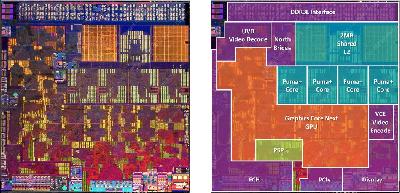
The AMD A8-6410 is a mobile quad-core SoC (codenamed "Beema") for entry-level devices and subnotebooks, which has been presented in spring 2014. In addition to 4 CPU cores clocked at 2.0 - 2.4 GHz (boost clock), the 28 nanometer chip also integrates a Radeon R5 GPU, a single-channel DDR3L-1866 memory controller and the Southbridge with various I/O-ports. Besides the slightly higher base clock (2.0 instead of 1.8 GHz), the technical data and therefore the performance is almost identical to the A6-6310 APU.
Architecture
Both Beema (for notebooks) and Mullins (for tablets and compact subnotebooks, same die) are based on AMD's Puma+ architecture, which is the successor to the previous Jaguar design (Kabini and Temash APUs). Neither the performance per clock nor the feature set (including SSE up to 4.2, AVX and AES) have been modified. However, AMD managed to reduce the leakage current, enabling significantly higher (boost) clock speeds. This leads to a more responsive system and better overall performance. As its predecessor, the chip is manufactured in 28 nm.
Performance
In single thread tasks, the A8-6410 is clearly faster than the former A6-5200 (25 W, 2.0 GHz), but just slightly ahead in multi thread benchmarks. Overall, the APU offers a performance similar to a Haswell-based Pentium or Core i3 (ULV). Nonetheless, the A8-6410 will be sufficient for all daily workloads like Office, Internet browsing and multimedia.
Graphics
The SoC integrates a Radeon R5 GPU with 128 shaders, which is based on the GCN architecture and clocked at up to 800 MHz. On average, the graphics performance is similar to Intel's HD Graphics 4200 or a dedicated Radeon HD 7470M. Only a few current games (as of 2014) are thus playable in low settings, but older and less demanding titels should run flawlessly.
Power Consumption
The power consumption of the entire SoC is rated at 15 watts. Thus, the APU is suitable for smaller subnotebooks.
AMD A4-6210
► remove from comparison
The AMD A4-6210 is a mobile quad-core SoC (codenamed "Beema") for entry-level devices and subnotebooks, which has been presented in April 2014. In addition to 4 CPU cores clocked at up to 1.8 GHz (no boost), the 28 nanometer chip also integrates a Radeon R3 GPU, a single-channel DDR3L-1600 memory controller and the Southbridge with various I/O-ports.
Architecture
Both Beema (for notebooks) and Mullins (for tablets and compact subnotebooks, same die) are based on AMD's Puma+ architecture, which is the successor to the previous Jaguar design (Kabini and Temash APUs). Neither the performance per clock nor the feature set (including SSE up to 4.2, AVX and AES) have been modified. However, AMD managed to reduce the leakage current, enabling significantly higher (boost) clock speeds. This leads to a more responsive system and better overall performance. As its predecessor, the chip is manufactured in 28 nm.
Performance
According to the clock rate, the APU is clearly faster than the former A4-5000 (15 W, 1.5 GHz), but somewhat slower than the A6-5200 (25 W, 2.0 GHz). Nonetheless, the A4-6210 will be sufficient for all daily workloads like Office, Internet browsing and multimedia.
Graphics
The SoC integrates a Radeon R3 GPU with 128 shaders, which is based on the GCN architecture and clocked at up to 600 MHz. On average, we expect the graphics performance to be similar to Intel's HD Graphics 4000 (ULV versions) or a Radeon HD 8400. Current games (as of 2014) are thus hardly playable even in low settings, but some older and less demanding titels will run flawless.
Power Consumption
The power consumption of the entire SoC is rated at 15 watts. Thus, the APU is suitable for smaller subnotebooks.
| Model | AMD A6-6310 | AMD A8-6410 | AMD A4-6210 | ||||||||||||||||||||||||||||||||||||
| Series | AMD A-Series | AMD A-Series | AMD A-Series | ||||||||||||||||||||||||||||||||||||
| Codename | Beema | Beema | Beema | ||||||||||||||||||||||||||||||||||||
| Series: A-Series Beema |
|
|
| ||||||||||||||||||||||||||||||||||||
| Clock | 1800 - 2400 MHz | 2000 - 2400 MHz | 1800 MHz | ||||||||||||||||||||||||||||||||||||
| L1 Cache | 256 KB | 256 KB | 256 KB | ||||||||||||||||||||||||||||||||||||
| L2 Cache | 2 MB | 2 MB | 2 MB | ||||||||||||||||||||||||||||||||||||
| Cores / Threads | 4 / 4 | 4 / 4 | 4 / 4 | ||||||||||||||||||||||||||||||||||||
| TDP | 15 Watt | 15 Watt | 15 Watt | ||||||||||||||||||||||||||||||||||||
| Transistors | 930 Million | 930 Million | |||||||||||||||||||||||||||||||||||||
| Technology | 28 nm | 28 nm | 28 nm | ||||||||||||||||||||||||||||||||||||
| Die Size | 107 mm2 | ||||||||||||||||||||||||||||||||||||||
| Features | SSE (1, 2, 3, 3S, 4.1, 4.2, 4A), x86-64, AES, AVX, Single-Channel DDR3L-1866 | MMX, SSE4.2, AES, AVX, BMI1, F16C, AMD64, VT | SSE (1, 2, 3, 3S, 4.1, 4.2, 4A), x86-64, AES, AVX, Single-Channel DDR3L-1600 | ||||||||||||||||||||||||||||||||||||
| iGPU | AMD Radeon R4 (Beema) (? - 800 MHz) | AMD Radeon R5 (Beema/Carrizo-L) (? - 800 MHz) | AMD Radeon R3 (Mullins/Beema) ( - 600 MHz) | ||||||||||||||||||||||||||||||||||||
| Architecture | x86 | x86 | x86 | ||||||||||||||||||||||||||||||||||||
| Announced | |||||||||||||||||||||||||||||||||||||||
| Socket | BGA769 |
