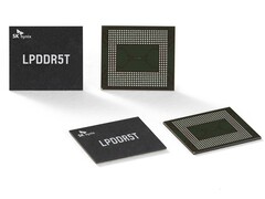
SK hynix has reportedly achieved a major milestone with an innovation that could change how mobile devices handle AI. The company’s new hybrid architecture, High-Bandwidth Storage (HBS), merges DRAM and NAND, enabling higher data speeds, lower latency, and improved energy efficiency.
According to ETNews, SK hynix expects its new tech to boost smartphone AI performance.
Next-gen memory for AI-powered mobile devices
The key part of SK hynix’s latest innovation is Vertical Wire Fan-Out (VFO) technology. VFO is a method that allows up to 16 layers of DRAM and NAND to be stacked vertically while they are connected in a straight line. With this process, SK hynix can reduce signal loss and transmission distance because there is no need for the curved wiring common in traditional packages.
The outcome is an HBS package with a shorter data processing time and increased efficiency. This brings bandwidth improvements to mobile devices, similar to how High-Bandwidth Memory (HBM) boosted performance in GPUs and AI servers.
Smaller, faster, and cooler
According to SK hynix, its new VFO process cuts wiring requirements by 4.6 times. It reduces power consumption by 5 percent and improves heat dissipation by 1.4 percent. The South Korean company also slashed the packaging height by 27 percent, allowing mobile devices to be even slimmer and to operate at lower temperatures.
SK hynix is also saving on production costs because HBS does not require Through-Silicon Via (TSV) manufacturing, which vertically connects stacked chips by drilling and filling microscopic holes through the silicon wafers, unlike HBM. In addition, this helps to increase yield, which is crucial for scaling production.
Bringing AI performance to mobile chips
When paired with the application processor (AP), SK hynix’s HBS module will enable smartphones and tablets to handle AI workloads better. The company has already used VFO-based DRAM packaging in Apple’s Vision Pro.


