SK hynix starts mass production of 321-layer 2-terabit QLC NAND
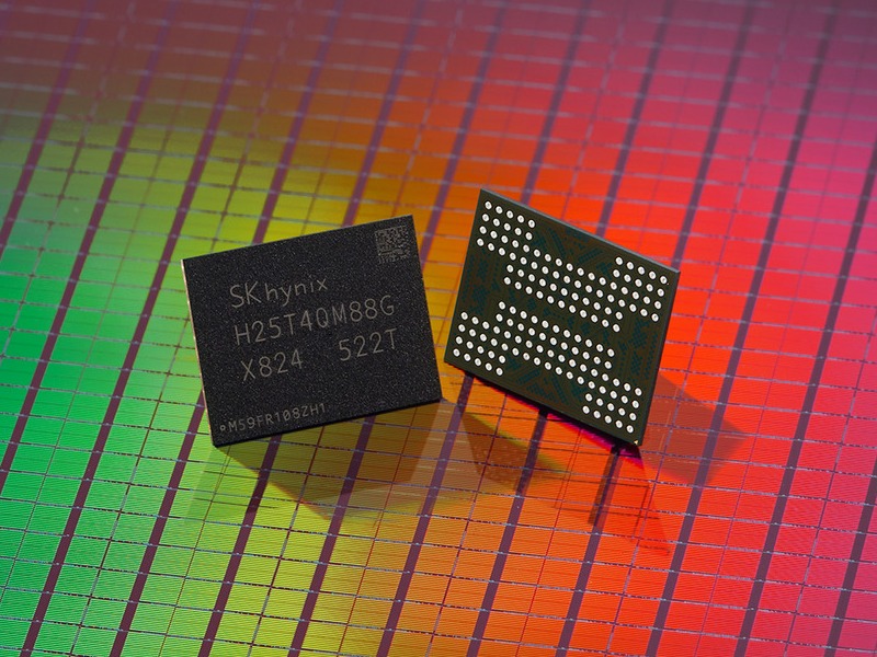
SK hynix has begun mass production of its 321-layer, 2-terabit (250 gigabytes) QLC NAND, claimed to be the first QLC device to break the 300-layer mark. First commercial products are slated for the first half of next year, pending customer validation.
The company doubled the per-die capacity compared to prior QLC generations and increased the number of planes inside each chip from four to six. More planes enable greater parallel processing, resulting in a significant increase in simultaneous read performance without compromising latency. SK hynix claims that the new QLC doubles data transfer speed, boosts write performance by up to 56 percent, and enhances read performance by 18 percent. Write power efficiency is also up by more than 23 percent, which matters for power-constrained AI data centers.
On the interface side, these V9Q dies operate at 3,200 mega-transfers per second, slightly below the high-end TLC NAND at 3,600 mega-transfers per second; however, the architectural improvements deliver substantial performance benefits for QLC workloads. The six-plane layout is the key enhancement here, and it's the main reason simultaneous read speeds improve.
Density brings additional benefits. A 2-terabyte client SSD can be built with only eight of these 2-terabit dies, cutting package count and bill of materials. SK hynix plans to start with PC SSDs, then expand to enterprise SSDs for data centers and UFS for phones as validation is completed.
For ultra-high capacities, the company's 32DP packaging can stack 32 dies in one package to maximize integration density. SK hynix points to an enterprise drive in development, targeting the 244-terabyte class, aimed at AI servers that require massive storage capacity with efficient power consumption for data center deployments.
Source(s)
SK hynix (in English)
