Review Intel Haswell Processors
For the original German article, see here.
The Processor market has always been a growing one with increasing sales figures year-over-year but that is changing pretty rapidly with a sharp down-trend observed in the last few quarters. In addition to the recent economic turbulence, especially in the Euro zone, the rapid growth of ARM devices has affected PC sales as well as other X86 based devices. Even the market leader Intel is not immune to this trend and its profits have dropped off substantially in the first quarter of 2013. The company is working hard in trying to find new growth areas to maintain their level of profitability. New products should be able to help Intel’s bottom line (to a certain extent) and maintain its lead over AMD.
Intel promises a lot with the Haswell architecture announced today. "The PC Re-Invented" is the trademark slogan of the marketing department. The focus is on the ever-shrinking form-factors like thin-and-lights, ultrabooks and the touch tablet (convertibles). Haswell aims to put out more CPU and GPU performance at much lower power consumption making the next generation of ultra-portable devices a much better proposition for the buyer.
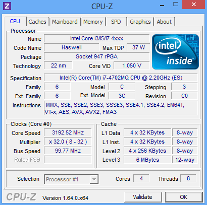
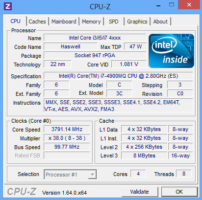
In this article, we will briefly describe the technical innovations and benchmark the five quad core models: Core i7-4702MQ, i7-4700MQ, i7-4800MQ, i7-4900MQ, and i7-4930MX. The performance of the integrated HD Graphics 4600 is covered in a special article:
Design
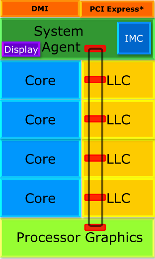
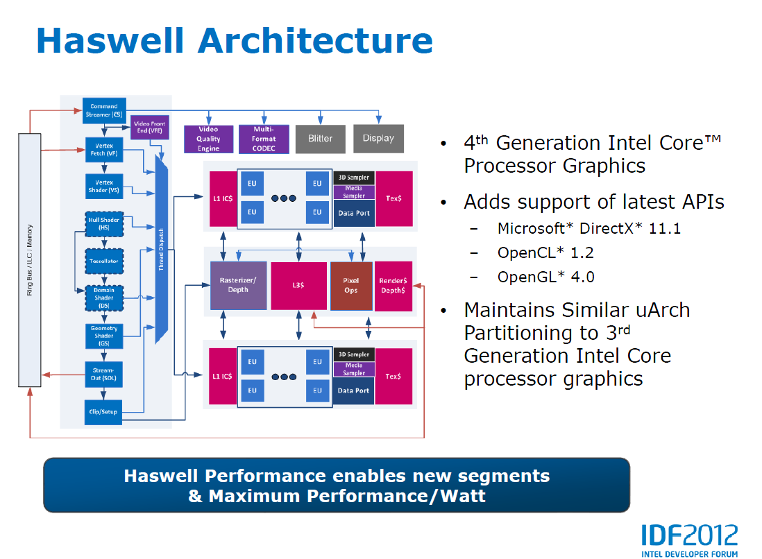
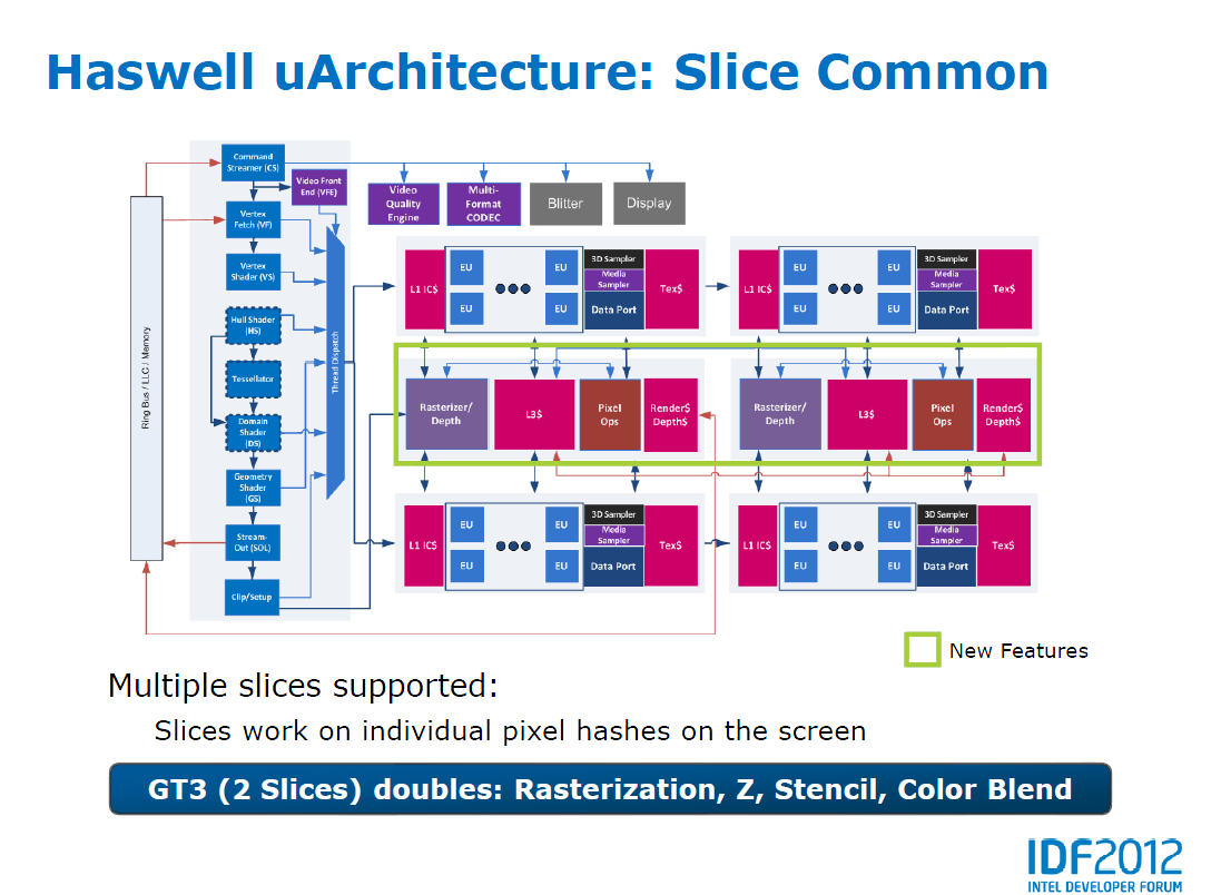
Before analyzing the CPU and GPU in detail, we would like to describe its design. The die shot Haswell consists of four components: processor, graphics unit, L3-/LLC-cache and the system agent (contains memory and display controller, DMI and I/O). These components are connected through a 256 bit ring bus introduced in Sandy Bridge. Despite many improvements, the die size of the quad core CPU with GT2 GPU of 177 mm² (Haswell) is only marginally bigger than the Ivy Bridge at 160 mm² which is pretty amazing and the number of transistors of about 1.4 billion remained about the same. The specifications of other models expected soon (quad core CPUs with GT3 GPU, dual core CPUs with GT2 or GT3 GPU, native GT1 models) are not known yet.
The technical specifications of quad-cores with GT2 graphics:
- 22 m Tri-Gate process
- 1.4 billion transistors
- 177 mm² die size
- 32 + 32 KB L1 cache for data and instructions (per core)
- 256 KB L2 cache (per core)
- up to 8 MB L3 cache (shared between CPU and GPU)
- MMX, SSE up to 4.2, AVX, AVX2, FMA3, AES-NI, Intel 64
- HD 4600 graphics unit (GT2, DirectX 11.1, 20 EUs)
- DDR3(L) memory controller up to 800 MHz (DDR3-1600)
- 16 Lanes to PCIe 3.0
- TDP of 37, 47 or 57 W
The processor is connected to the chipset via the well-known DMI (Direct Media Interface) code named "Lynx Point" for the Haswell platform. The biggest change is the more advanced 32 nm process, which promises less energy consumption than the 65 nm "Panther Point" (Ivy Bridge chip sets). For the moment, HM86, HM87, and the business version QM87 will be launched for notebooks. Unfortunately, we do not know detailed specifications of the models yet. But, with up to 6x USB 3.0 and 6x SATA-III (Panther Point: 4x USB 3.0, 2x SATA-III) they bring several improvements over the last generation.
CPU
Since 2007, Intel's developers have followed the "Tick-Tock" model. Every year - neglecting small delays - a die shrink of the process technology ("tick") follows a micro-architectural change ("tock"). Ivy Bridge was a slightly modified die shrink of the Sandy Bridge generation, while Haswell is a new architecture in the same 22 nm process.
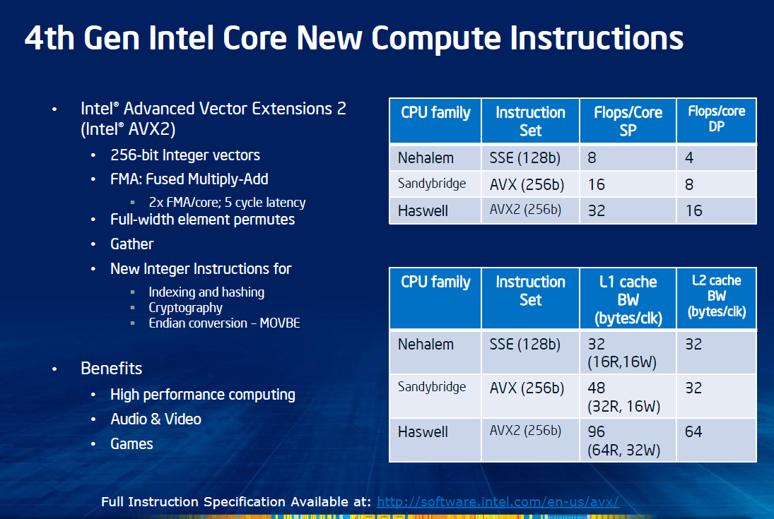
But Haswell is not a completely new architecture and has many features found in Ivy Bridge. Nevertheless, there are several important changes: The additional instruction set extension AVX2 and FMA3, BMI (Bit Manipulation Instructions) and TSX (Transactional Synchronization Extensions) to name a few. While AVX2 in simple speak, a kind of integer extension of the first AVX generation, FMA3 adds several new instructions for floating point code with 128 and 256 bit operands. Please note that FMA3 is not directly compatible with FMA4, which is already supported by the latest AMD processors (Trinity, Richland) in addition to FMA3. The crucial difference is the way the registers are used. FMA4 allows FMA operations like "a + (b * c) = d", while the destination register "d" must be one of the three registers "a", "b", or "c" in FMA3. The two other extensions improve cryptography tasks (BMI) or optimize the synchronization of parallel threads (TSX).
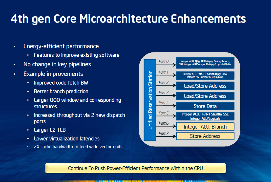
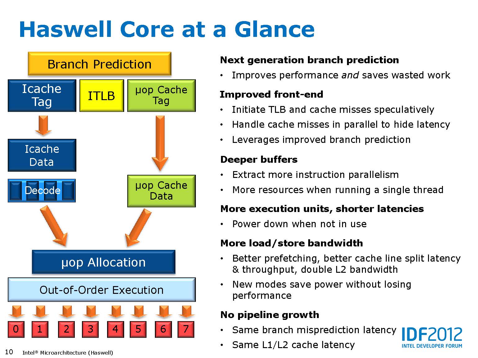
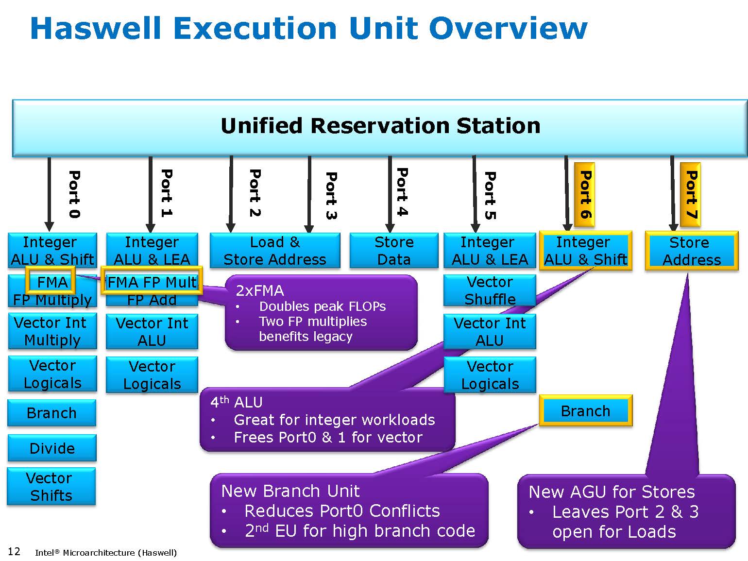
The pipeline still has 14 to 19 levels (the actual length depends on the hit rate of the µOP cache) and shows that Intel has made only small changes. The engineers haven’t changed the front-end. They only improved the prefetcher and optimized the jump prediction. Meanwhile, the back-end has been extensively modified. Bigger Buffers like an ROB (Reorder Buffer, also called OoO window) with 168 instead of 192 µOPs improves the flexibility and the efficiency of out-of-order scheduling. In addition, the number of execution units was increased from 6 to 8. Especially the latter is a big difference of Haswell over its predecessors. All "Core" architectures since Conroe, better known as first generation of the Core 2 Duo could only execute 6 µOPs in parallel. This change should especially pay off in combination with SMT - a single thread will rarely be able to use all available units.
If the pipeline does not get data quickly enough, the throughput drops. In order to avoid a bottleneck, Intel did not only double the size of the L2 TLB, but also widened the interface of the L1 and L2 caches by doubling it. The bandwidth of the single parts of the L3-Cache (LLC) shared between all cores was increased by means of two dedicated pipelines for data and other operations. At the same time the flexibility was improved. While the LLC was in the same clock domain as the CPU cores in Ivy Bridge, Haswell allows for independent clocking. This is particularly useful in graphics applications. If the GPU load is high and the CPU load low, the processor cores run at a lower clock rate and save energy while the graphics unit still profits from the full speed of the cache.
To summarize, the changes of Haswell will lead to significant performance gains. Apart from coming software with support to the new instruction set extensions, existing applications will profit to a certain extent. At the same time, the energy efficiency has been improved. A more sophisticated Power Gating disconnects components not used from the power supply. Furthermore, switching between the different power states has gotten faster by about 25 percent and ULV models feature a new, extremely frugal S0ix mode.
GPU
Intel delayed a radical GPU redesign until Haswell’s successor, Broadwell. Nevertheless, the performance gain of the GPU is significantly bigger than the CPU's.
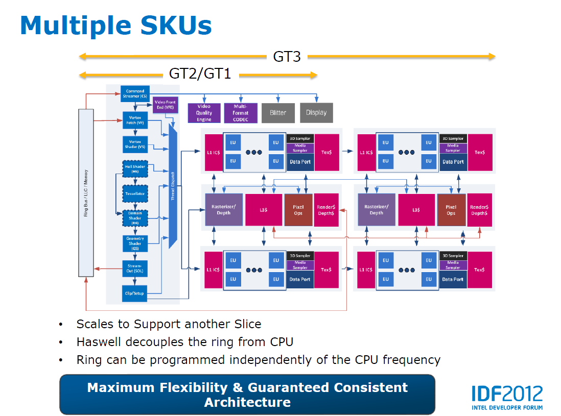
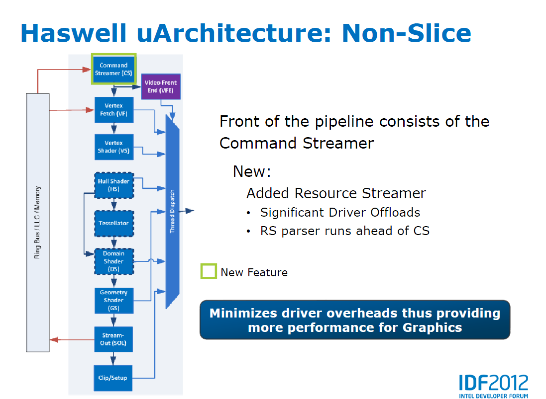
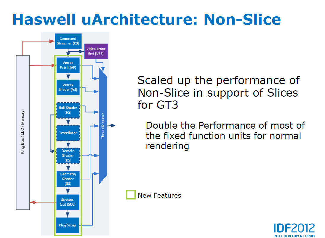
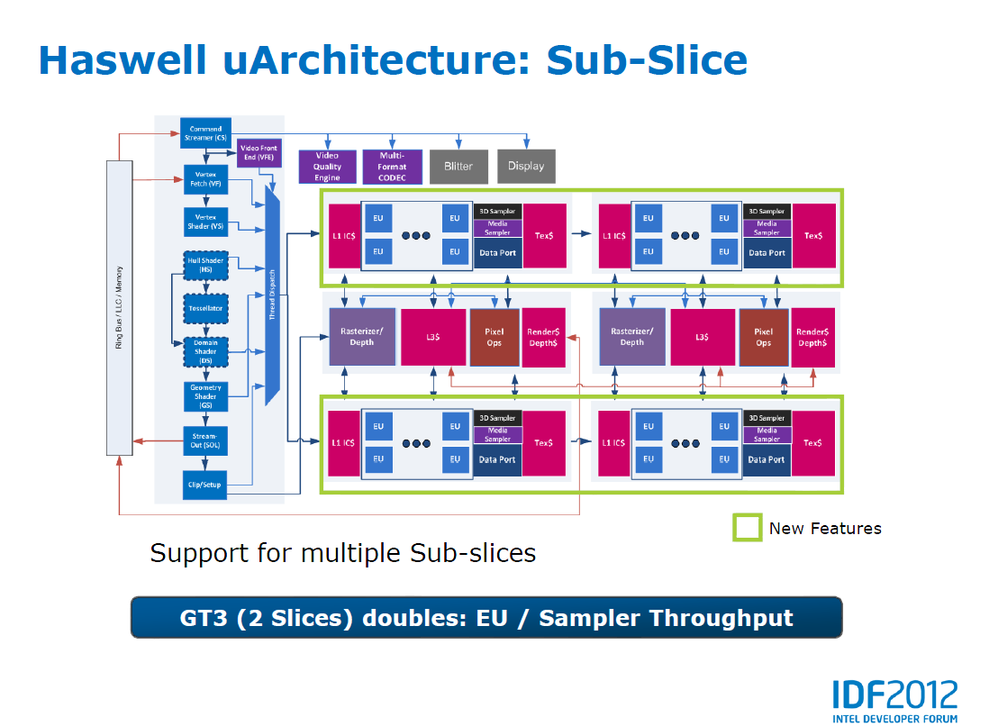
This was made possible by adding significantly more shader units called "Execution Units" (EUs) by Intel. Instead of 6 (GT1) or 16 EUs (GT2) in Ivy Bridge, the Haswell GPU features 10 (GT1), 20 (GT2) and 40 (GT3) EUs. All models have a slightly redesigned front-end in common, which includes the new Resource Streamer (part of the Command Streamer which reduces the driver overhead) and well known components like the Tessellator. These and other fixed function units should be twice as fast as its predecessor.
These are followed by the actual execution units, which are split into scalable slices. A slice consists of a separate L3 cache for the GPU, the pixel back end, and the Rasterizer. In addition, there are one (GT1) or two (GT2) sub-slices. Each one consists of 10 EUs, an instruction memory and a radically redesigned texture sampler with four times the throughput of Ivy Bridge's. The GT3-GPU features two slices and four sub-slices and 40 shaders units (EUs).
The top version of the graphics unit (GT3e) additionally features 128 MB eDRAM cache directly beside the chip in the same package. Thanks to an extremely wide 512 bit interface – RAM is usually only connected via two 64 bit channels - the bandwidth of the GPU is very large. At a clock rate of - say - 500 MHz (very careful estimation), it has a throughput of at least 64 GB/s and is on par with Nvidia's GeForce GT 650M with GDDR5 memory. However, it remains to be seen whether the low capacity of the eDRAMs can really keep up with the video memory of a dedicated GPU. In addition, the graphics unit use its dedicated L3 cache (see above), the LLC of up to 8 MB and the DDR3 RAM of the system.
We also want to briefly mention another feature of the eDRAM here. According to Intel, it can not only be used by the GPU, but also by the CPU cores. So, you could also call it a very big "off-die" L4 cache. This could bring same performance advantages in special tasks which depend heavily on bandwidth. However, we need to wait for the first benchmarks of these models (Core i7-4850HQ, Core i7-4950HQ) to analyze this.
There were also several changes in the feature-set of the GPUs. Haswell supports all important APIs like DirectX 11.1, OpenGL 4.0, and OpenCL 1.2 now. So, you can use the GPU for GPGPU purposes which pays off in several existing applications like Adobe Photoshop and Premiere Pro and any future software using these technologies. The graphics chip can still drive up to three displays in different configurations with a maximum resolution of 4k x 2k (see the following figures for details). The available interfaces are HDMI 1.4a and DisplayPort 1.2 which inludes Daisy Chaining. However, only non-ULV models support VGA. The new Wireless Display version 4.1, allows a wireless transmission of the signal and promises reduced delays in latency for critical applications like games. Finally, the Quick-Sync transcoder has also been redesigned and its performance improved.
Overview of the models
Today Intel officially introduces five new quad core processors, three models of the M series (Core i7-4930MX, i7-4900MQ, and i7-4800MQ) and two models of the H series (Core i7-4950HQ, i7-4850HQ).
The mobile chips that include the Core i7-4930MX (the fastest chip in the roster) directly replace all the processors from the Ivy Bridge generation with similar clocks and L3 cache. They use the medium GT2 GPU configuration called HD Graphics 4600.
Meanwhile, the HQ models are completely new. Although the model number would suggest higher performance (e.g. Core i7-4950HQ vs. i7-4900MQ), their CPU clock is 200 to 400 MHz lower, but they feature the fast GT3e GPU Iris Pro Graphics 5200 which makes them very expensive. A surcharge of just under $100 USD compared to the MQ model with a faster CPU is quite steep.
In addition to these models, several models for OEM manufacturers will also be released - like the Core i7-4700MQ, the successor of the popular Core i7-3630QM. With the Core i7-4702MQ, Intel again offers an especially frugal chip with a 37 W TDP for smaller notebooks. Both chips will also be available as HQ models with support for vPro, but unfortunately without the Iris Pro GPU. Only the Core i7-4750HQ will offer the fastest graphics solution.
| Name | # of cores | base clock | Turbo QC / DC / SC | L3 cache | TDP | GPU clock | price |
|---|---|---|---|---|---|---|---|
| M series (HD Graphics 4600) | |||||||
| Core i7-4930MX | 4/8 | 3.0 GHz | 3.7 / 3.8 / 3.9 GHz | 8 MB | 57 W | 400-1350 MHz | 1096 $ |
| Core i7-4900MQ | 4/8 | 2.8 GHz | 3.6 / 3.7 / 3.8 GHz | 8 MB | 47 W | 400-1300 MHz | 568 $ |
| Core i7-4800MQ | 4/8 | 2.7 GHz | 3.5 / 3.6 / 3.7 GHz | 6 MB | 47 W | 400-1300 MHz | 378 $ |
| Core i7-4700MQ | 4/8 | 2.4 GHz | 3.2 / 3.3 / 3.4 GHz | 6 MB | 47 W | 400-1150 MHz | OEM |
| Core i7-4702MQ | 4/8 | 2.2 GHz | 2,9 / 3.1 / 3.2 GHz | 6 MB | 37 W | 400-1150 MHz | OEM |
| H series (Iris Pro Graphics 5200) | |||||||
| Core i7-4950HQ | 4/8 | 2.4 GHz | 3.4 / 3.5 / 3.6 GHz | 6 MB | 47 W | 200-1300 MHz | 657 $ |
| Core i7-4850HQ | 4/8 | 2.3 GHz | 3.3 / 3.4 / 3.5 GHz | 6 MB | 47 W | 200-1300 MHz | 468 $ |
| Core i7-4750HQ | 4/8 | 2.0 GHz | 3.0 / 3.1 / 3.2 GHz | 6 MB | 47 W | 200-1200 MHz | OEM |
| H series (HD Graphics 4600) | |||||||
| Core i7-4700HQ | 4/8 | 2.4 GHz | 3.2 / 3.3 / 3.4 GHz | 6 MB | 47 W | 400-1200 MHz | OEM |
| Core i7-4702HQ | 4/8 | 2.2 GHz | 2.9 / 3.1 / 3.2 GHz | 6 MB | 37 W | 400-1150 MHz | OEM |


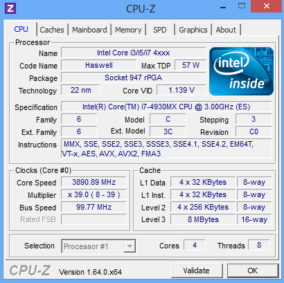
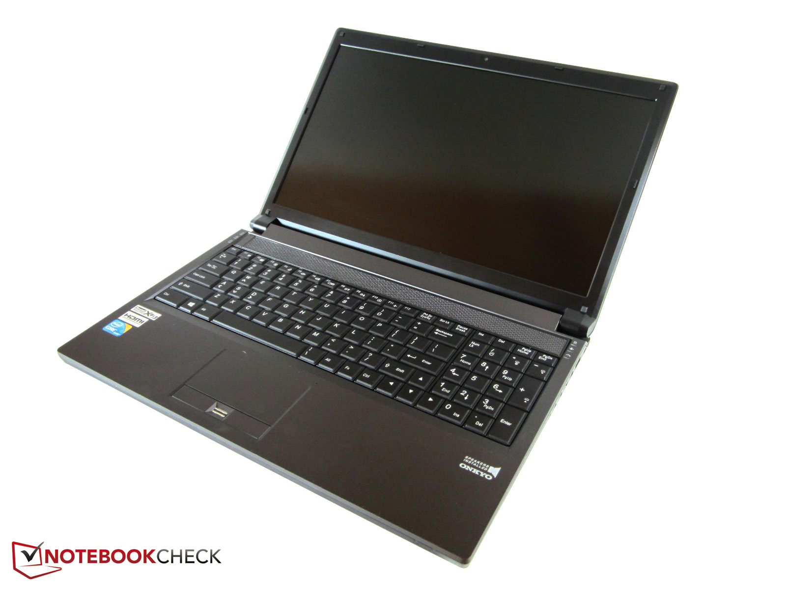
The test system
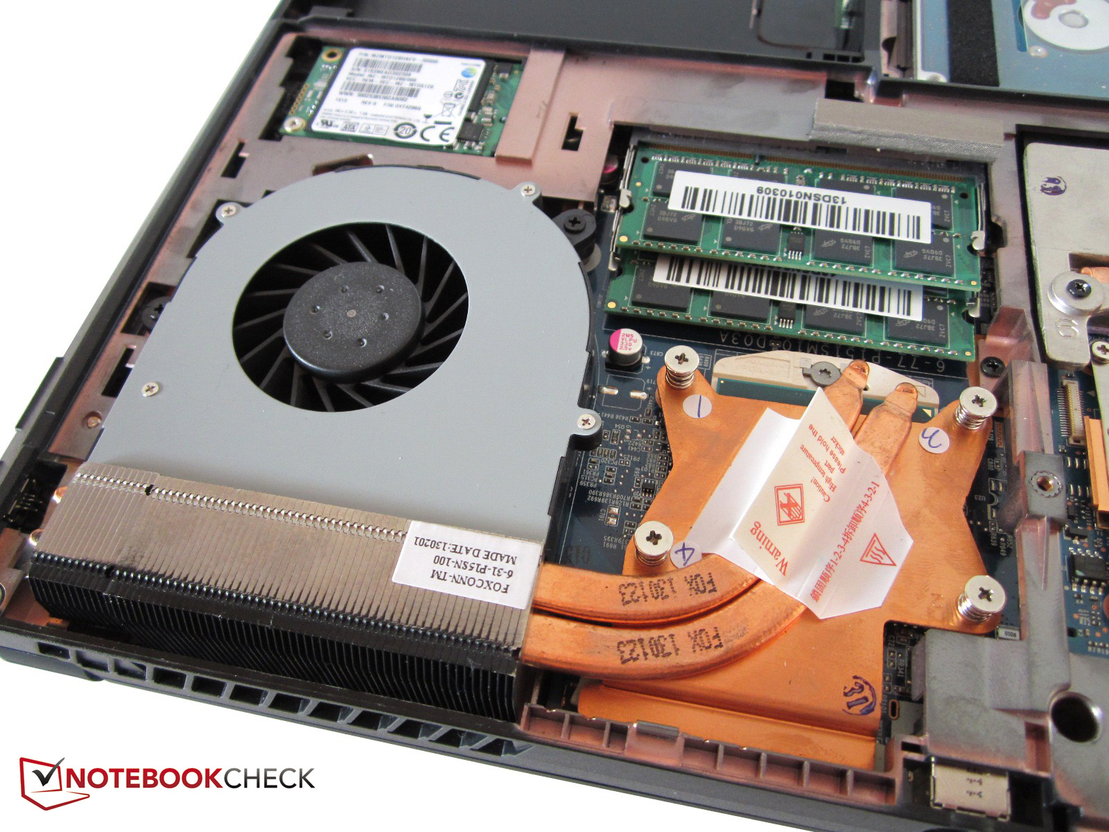
Schenker kindly made a barebone available to us for our CPU tests. The Clevo P150SM, which Schenker sells under the name W503, features an especially powerful cooling system which can also keep top-end processors like the Core i7-4930MX with a 57 W TDP in check.
In addition to this, the test system featured 2x 4 GB DDR3-1600 RAM, a 128 GB mSATA SSD from Samsung, and a large 180 W power adapter. The built-in graphics card, a GeForce GTX 765M, was deactivated in favor of the integrated HD Graphics 4600 for all measurements.
Detailed information about the notebook, benchmarks with dedicated graphics card, etc. are available in our in-depth review:
Test configuration:
- Intel Haswell Quad-Core Processors (ES)
- Intel HM87 chip set
- 2x 4 GB Micron DDR3-1600 RAM (CL11)
- HD Graphics 4600
- Samsung SSD PM841 (mSATA, 128 GB)
- 180 W power adapter
- Windows 8 Enterprise 64 Bit
Benchmarks
Before we come to the results, we have to mention a limitation of our test system. The Clevo P150SM and other Haswell barebones from the Taiwanese manufacturer still had problems allowing the maximum Turbo frequency to be reached during multi-threaded operations at the time of testing. In our case, the Core i7-4800MQ, the 4900MQ, and the 4930MX were limited to a maximum of 3.4 GHz. As a result the performance is 3 to 9 percent lower and we hope that this problem will be solved in the final devices. We have still mentioned the results even with this problem. At least, they allow for a rough classification of the Haswell CPUs. We had no issues with the single-threaded tests with maximum Turbo frequencies possible with the device.
| Cinebench R11.5 | |
| CPU Multi 64Bit (sort by value) | |
| Core i7-4930MX (Clevo P150SM) | |
| Core i7-4900MQ (Clevo P150SM) | |
| Core i7-4800MQ (Clevo P150SM) | |
| Core i7-4700MQ (Clevo P150SM) | |
| Core i7-4702MQ (Clevo P150SM) | |
| One M73-2N, Ivy Bridge | |
| One M73-2N, Ivy Bridge | |
| One M73-2N, Ivy Bridge | |
| One M73-2N, Ivy Bridge | |
| CPU Single 64Bit (sort by value) | |
| Core i7-4930MX (Clevo P150SM) | |
| Core i7-4900MQ (Clevo P150SM) | |
| Core i7-4800MQ (Clevo P150SM) | |
| Core i7-4700MQ (Clevo P150SM) | |
| Core i7-4702MQ (Clevo P150SM) | |
| One M73-2N, Ivy Bridge | |
| One M73-2N, Ivy Bridge | |
| One M73-2N, Ivy Bridge | |
| One M73-2N, Ivy Bridge | |
| X264 HD Benchmark 4.0 | |
| Pass 2 (sort by value) | |
| Core i7-4930MX (Clevo P150SM) | |
| Core i7-4900MQ (Clevo P150SM) | |
| Core i7-4800MQ (Clevo P150SM) | |
| Core i7-4700MQ (Clevo P150SM) | |
| Core i7-4702MQ (Clevo P150SM) | |
| One M73-2N, Ivy Bridge | |
| One M73-2N, Ivy Bridge | |
| One M73-2N, Ivy Bridge | |
| One M73-2N, Ivy Bridge | |
| Pass 1 (sort by value) | |
| Core i7-4930MX (Clevo P150SM) | |
| Core i7-4900MQ (Clevo P150SM) | |
| Core i7-4800MQ (Clevo P150SM) | |
| Core i7-4700MQ (Clevo P150SM) | |
| Core i7-4702MQ (Clevo P150SM) | |
| One M73-2N, Ivy Bridge | |
| One M73-2N, Ivy Bridge | |
| One M73-2N, Ivy Bridge | |
| One M73-2N, Ivy Bridge | |
| TrueCrypt | |
| Serpent Mean 100MB (sort by value) | |
| Core i7-4930MX (Clevo P150SM) | |
| Core i7-4900MQ (Clevo P150SM) | |
| Core i7-4800MQ (Clevo P150SM) | |
| Core i7-4700MQ (Clevo P150SM) | |
| Core i7-4702MQ (Clevo P150SM) | |
| One M73-2N, Ivy Bridge | |
| One M73-2N, Ivy Bridge | |
| One M73-2N, Ivy Bridge | |
| One M73-2N, Ivy Bridge | |
| Twofish Mean 100MB (sort by value) | |
| Core i7-4930MX (Clevo P150SM) | |
| Core i7-4900MQ (Clevo P150SM) | |
| Core i7-4800MQ (Clevo P150SM) | |
| Core i7-4700MQ (Clevo P150SM) | |
| Core i7-4702MQ (Clevo P150SM) | |
| One M73-2N, Ivy Bridge | |
| One M73-2N, Ivy Bridge | |
| One M73-2N, Ivy Bridge | |
| One M73-2N, Ivy Bridge | |
| AES Mean 100MB (sort by value) | |
| Core i7-4930MX (Clevo P150SM) | |
| Core i7-4900MQ (Clevo P150SM) | |
| Core i7-4800MQ (Clevo P150SM) | |
| Core i7-4700MQ (Clevo P150SM) | |
| Core i7-4702MQ (Clevo P150SM) | |
| One M73-2N, Ivy Bridge | |
| One M73-2N, Ivy Bridge | |
| One M73-2N, Ivy Bridge | |
| One M73-2N, Ivy Bridge | |
| WinRAR - Result (sort by value) | |
| Core i7-4930MX (Clevo P150SM) | |
| Core i7-4900MQ (Clevo P150SM) | |
| Core i7-4800MQ (Clevo P150SM) | |
| Core i7-4700MQ (Clevo P150SM) | |
| Core i7-4702MQ (Clevo P150SM) | |
| One M73-2N, Ivy Bridge | |
| One M73-2N, Ivy Bridge | |
| One M73-2N, Ivy Bridge | |
| One M73-2N, Ivy Bridge | |
| 3DMark 06 - CPU - CPU Score (sort by value) | |
| Core i7-4930MX (Clevo P150SM) | |
| Core i7-4900MQ (Clevo P150SM) | |
| Core i7-4800MQ (Clevo P150SM) | |
| Core i7-4700MQ (Clevo P150SM) | |
| Core i7-4702MQ (Clevo P150SM) | |
| One M73-2N, Ivy Bridge | |
| One M73-2N, Ivy Bridge | |
| One M73-2N, Ivy Bridge | |
| One M73-2N, Ivy Bridge | |
| 3DMark Vantage - 1280x1024 P CPU no PhysX (sort by value) | |
| Core i7-4930MX (Clevo P150SM) | |
| Core i7-4900MQ (Clevo P150SM) | |
| Core i7-4800MQ (Clevo P150SM) | |
| Core i7-4700MQ (Clevo P150SM) | |
| Core i7-4702MQ (Clevo P150SM) | |
| One M73-2N, Ivy Bridge | |
| One M73-2N, Ivy Bridge | |
| One M73-2N, Ivy Bridge | |
| One M73-2N, Ivy Bridge | |
| 3DMark 11 - 1280x720 Performance Physics (sort by value) | |
| Core i7-4930MX (Clevo P150SM) | |
| Core i7-4900MQ (Clevo P150SM) | |
| Core i7-4800MQ (Clevo P150SM) | |
| Core i7-4700MQ (Clevo P150SM) | |
| Core i7-4702MQ (Clevo P150SM) | |
| One M73-2N, Ivy Bridge | |
| One M73-2N, Ivy Bridge | |
| One M73-2N, Ivy Bridge | |
| One M73-2N, Ivy Bridge | |
Because of the aforementioned turbo problem, our results are not a clear representation of the capabilities of the Haswell platform. We were very impressed by the three fastest chips which matched the performance figures of the Core i7-3940XM which is clocked about 200-300 MHz higher. The performance-per-MHz increased by about 10 percent on average. In the single threaded test of Cinebench R11.5 (maximum turbo can be reached) the Core i7-4930MX is 7 percent faster than the fastest chip last year. If you take the different clock rates into account, the performance gain is about the same in most other applications. But we need to mention that we did not see any significant improvements in the Hyper-Threading technology.
However, performance gain smaller than 10 percent is still very small. But, you cannot expect more from this architecture without significantly changing the process or using much higher frequencies. We will probably have to accept that the performance per core will only marginally increase in the coming years.
At least the buyer gets the performance of a significantly more expensive Ivy Bridge CPU for the same price - and we did not consider the new instruction set extension of the Haswell models here. The difference might be significantly bigger in newer software which supportsAVX2 etc.
Power consumption
Due to the new socket of the Haswell CPUs, we had to use a different test system and cannot directly compare the power consumption with Ivy Bridge. In addition, we have to mention the turbo problem again. It does not only have an impact on performance, but also on power consumption. Therefore, we also mention the used frequencies in all following measurements.
Like in the previous tests, we have been able to measure the total power draw only. We will not be able to specifically evaluate the relative power-draws in absolute values but we will try to give you a picture of the extent of energy consumption improvements in the platform by eliminating as many variables as possible.
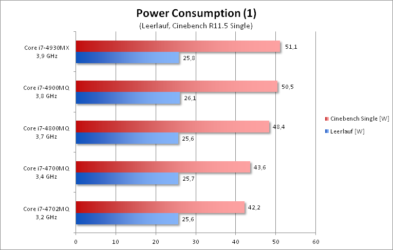
For the best possible comparison, all measurements of the energy demand were done with maximum display brightness, active WLAN, and the energy profile "maximum performance". While idle, the power consumption is rather high at about 26 W, but the chips do not differ much. Thanks to sophisticated energy saving mechanisms, the power consumption of all five CPUs is identical excluding measurement inaccuracies.
However, there are small differences during the single thread test of Cinebench R11.5. The energy demand climbs by about 1 to 2 W per 100 MHz frequency increase. The difference between the Core i7-4702MQ and the i7-4930MX is just under 9 W. In consideration of the small performance difference, it gets apparent that the energy efficiency massively decreases at frequencies nearing 4 GHz.
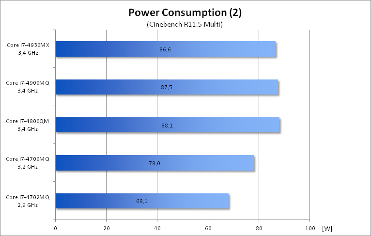
As the frequencies of the three fastest CPUs are limited to 3.4 GHz in the multi-threaded test in Cinebench, their power consumption is nearly identical. Only the 3.2 GHz Core i7-4700MQ requires about 9 W less. But, this high-end quad core CPU is also not really frugal. Therefore, Intel developed the i7-4702MQ with a TDP of 68 W (10 W less) for smaller, slimmer systems.
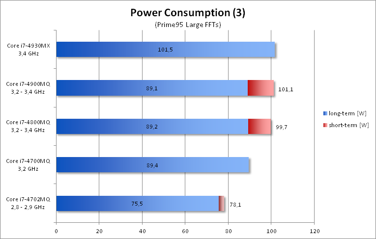
The maximum power consumption is measured during the synthetic stress test with Prime95. At the beginning of the test all models run at their maximum frequencies (multi thread)of 2.9, 3.2, or 3.4 GHz. But, the Core i7-4900MQ, the i7-4800MQ, and the i7-4702MQ exceed the maximum TDP specified by the manufacturer in these conditions. We already know this (intended) behavior first observed in the Sandy and Ivy Bridge. After an interval of about 30 seconds, the PCU (Power Control Unit) integrated into the CPU decreases the clock until the permitted TDP is again reached. So, the best possible performance is achieved without demanding too much from the thermal capacities of a notebook.
Meanwhile, the Core i7-4930MX and the 4700MQ have constant frequencies throughout the test. For the 4930MX, this is because of its high TDP of 57 W and the 3.4 GHz turbo limitation of the Clevo barebone. The slowest 4700MQ never exceeded the maximum TDP of 47 W during any of the tests.
The simultaneous stress on the CPU and GPU with Prime95 and FurMark is an exception. The power consumption only increases slightly, but a part of the TDP capacity is used for the graphics unit. Depending on the classification, we measured CPU/GPU frequencies of about 2.2/1.1 GHz (37 W model), 2.7/1.1 GHz (47 W models) and 3.0/1.2 GHz (57 W model).
Verdict
Is this a big change or an unnecessary update? In consideration of the performance, some might doubt that Intel's new architecture is a success. The performance gain is surely too small when running existing software to justify migrating from a Sandy Bridge or an Ivy Bridge CPU. At least this is true for the quad cores reviewed here.
We should not forget about the fact that the last few generations have featured fast processors. Although Intel's tick tock model ensures that the performance gain from generation to generation is only small, the updates bring constant improvement every year. AMD simply cannot compete with the CPU performance of the latest chips with their best performing mobile chips matching the Core i3s at best. In addition, Haswell features like AVX2 and FMA are mainly designed for future applications which could greatly profit from the new instruction set extension.
It could get exiting again when Intel introduces new Ultrabook models soon. Some interesting details already leaked include the modern 1-chip design; TDP reduced to 15 W and a significantly faster graphics unit. Our feature article about the HD Graphics 4600, the mid-level configuration ("GT2") of the Haswell graphics, gives us a taste of what is to come.
Many thanks to Schenker who made this review possible. You can configure your own Schenker here.
Sources
