Possible block diagram for Intel Gemini Lake leaks out
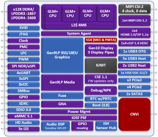
What looks to be an authentic block diagram of Intel’s yet-to-be-released Gemini Lake SoC has surfaced. Although not one of Intel’s high-end chips, it will play a key role in the embedded 2-in-1 market when it launches in (expectedly) Q4 this year. The successor to the Apollo Lake series, the Gemini Lake chips will bring improved performance-per-watt thanks in large part to Intel moving fabrication to its new 14nm process.
Importantly, Gemini Lake is also equipped with Intel’s Gen9LP GPU, with up to 18 execution units for improved graphics performance. While likely offering some hope for casual gamers and little else, it will be sufficient to drive high-resolution displays or monitors with native support for HDMI 2.0 also in tow. The block diagram also shows support for up to 5 USB 3.0 ports, 2 USB 2.0 ports and one USB 3.0 OTG port. PCIe, SATA 3 and eMMC 5.1 interconnect is also on offer, although UFC support still seems elusive.
According to a previously leaked Intel roadmap, Gemini Lake chips will be formally announced and begin to appear in shipping devices sometime in Q4 2017.

Source(s)
