

Apple M2 Max vs Intel Core 2 Duo P7370 vs Intel Core 2 Duo T9900
Apple M2 Max
► remove from comparison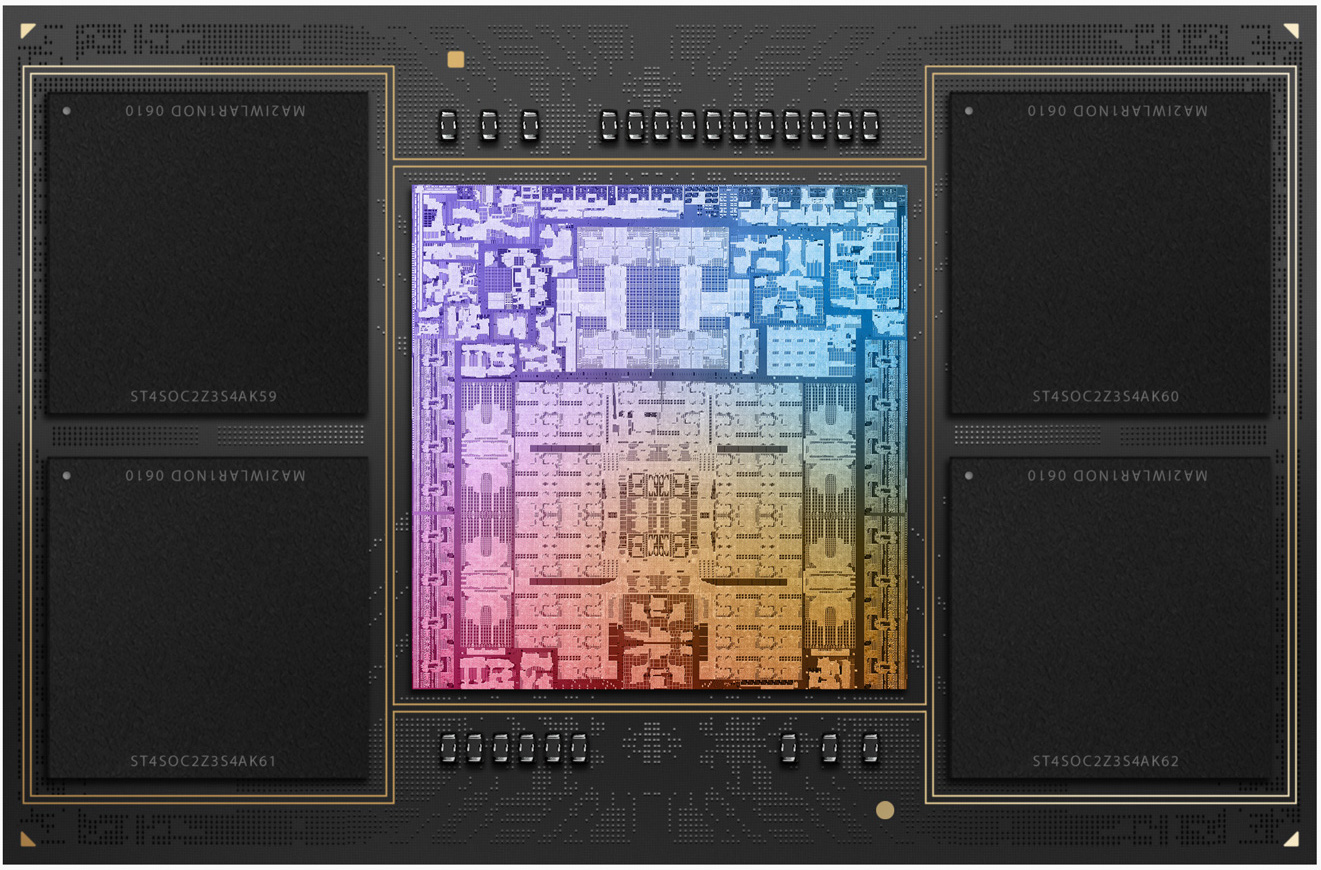
The Apple M2 Max is a System on a Chip (SoC) from Apple that is found in the early 2023 MacBook Pro 14 and 16-inch models. It offers all 12 CPU cores available in the chip divided in eight performance cores (P-cores) and four power-efficiency cores (E-cores). The E-cores clock with up to 3.4 GHz, the P-Cores up to 3.7 GHz (mostly 3.3 GHz in multi-threaded workloads and 3.4 GHz in single threaded).
The big cores (codename Avalanche) offer 192 KB instruction cache, 128 KB data cache, and 36 MB shared L2 cache (up from 24 MB in the M1 Pro). The four efficiency cores (codename Blizzard) are a lot smaller and offer only 128 KB instruction cache, 64 KB data cache, and 4 MB shared cache. CPU and GPU can both use the 49 MB SLC (System Level Cache).
The unified memory (32, 64, or 96 GB LPDDR5-6400) next to the chip is connected by a 512 Bit memory controller (400 GB/s bandwidth) and can be used by the GPU and CPU.
The CPU performance should be quite similar to the M2 Pro as only the higher memory bandwidth and bigger L3 cache could make a difference for some workloads.
The integrated graphics card in the M1 Max offers a 30-core GPU or a GPU with all 38 cores.
Furthermore, the SoC integrates a fast 16 core neural engine (faster than M1 Max), a secure enclave (e.g., for encryption), a unified memory architecture, Thunderbolt 4 controller, an ISP, and media de- and encoders (including ProRes).
The M2 Max is manufactured in 5 nm at TSMC (second generation) and integrates 40 billion transistors. The power consumption of the CPU part is up to 36 Watt according to powermetrics. When fully loading the CPU and GPU cores, the chip uses up to 89 Watt and the CPU part is limited to 25 Watt.
Intel Core 2 Duo P7370
► remove from comparisonThe Intel Core 2 Duo P7370 is a dual core processor for laptops. It features 2.0 GHz and a shared level 2 cache of 3 MB. It is based on the 45nm Penryn core, but most likely Trusted Execution and Virtualization (VT-x) are disabled.
The P7370 uses a Penryn (Montevina Update) core that features 2 integer units, 1 floating point unit, 1 load unit, and 1 store unit in a 14-stages long pipeline. Due to the Wide Dynamic Execution Technology, the core is able to simultaneously execute up to four instructions.
The integrated Enhanced Speedstep is able to downclock the core dynamically as low as 800 MHz to save power (in idle mode).
Intel Core 2 Duo T9900
► remove from comparison
The Intel Core 2 Duo T9900 is the theoretical successor of the Core 2 Extreme X9100 (which also clocks at 3.06 GHz) that uses less power due to the modern stepping and the Enhanced Halt State (C1E). The only advantage of the X9100 is the free multiplikator (which allows easy overclocking of the CPU).
The T9900 is a fast dual core CPU for laptops which features 6 MB of shared level 2 cache and a TDP of 35 Watt. Due to the high clock speed, modern games (in 2009) should not be limited by the CPU speed. For single threaded applications it is one of the fastest CPUs for laptops (only beaten by the new Core i7 with enabled Turbo mode).
The T9900 uses a Penryn (Montevina Update) core that features 2 integer units, 1 floating point unit, 1 load unit, and 1 store unit in a 14-stages long pipeline. Due to the Wide Dynamic Execution Technology, the core is able to simultaneously execute up to four instructions.
The integrated Enhanced Speedstep is able to downclock the core dynamically as low as 800 MHz to save power (in idle mode).
The Core 2 Duo T9900 can be used in a Socket P socket with 479 pins: Socket P / Micro Flip-Chip Pin Grid Array (Micro-FCPGA) requires 479-pin surface mount Zero Insertion Force (ZIF) socket (mPGA479M socket) or Micro Flip-Chip Ball Grid Array (Micro-FCBGA) for surface mount (479-ball).
| Model | Apple M2 Max | Intel Core 2 Duo P7370 | Intel Core 2 Duo T9900 | ||||||||||||||||
| Series | Apple M2 | Intel Core 2 Duo | Intel Core 2 Duo | ||||||||||||||||
| Series: Core 2 Duo Penryn |
| ||||||||||||||||||
| Clock | 2424 - 3696 MHz | 2000 MHz | 3060 MHz | ||||||||||||||||
| L1 Cache | 3.3 MB | 128 KB | |||||||||||||||||
| L2 Cache | 36 MB | 3 MB | 6 MB | ||||||||||||||||
| L3 Cache | 48 MB | ||||||||||||||||||
| Cores / Threads | 12 / 12 | 2 / 2 | 2 / 2 | ||||||||||||||||
| TDP | 79 Watt | 25 Watt | 35 Watt | ||||||||||||||||
| Transistors | 67000 Million | 410 Million | |||||||||||||||||
| Technology | 5 nm | 45 nm | 45 nm | ||||||||||||||||
| Features | ARMv8 Instruction Set | SSE4.1, Virtualization Technology, Execute Disable Bit, Enhanced Speedstep, Ehnaced Halt State (C1E), 64 Bit, Trusted Execution Technology | |||||||||||||||||
| iGPU | Apple M2 Max 38-Core GPU | ||||||||||||||||||
| Architecture | ARM | x86 | x86 | ||||||||||||||||
| Announced | |||||||||||||||||||
| Codename | Penryn | Penryn | |||||||||||||||||
| FSB | 1066 | 1066 | |||||||||||||||||
| Voltage | 1.05-1.2125 V V | ||||||||||||||||||
| Die Size | 107 mm2 | ||||||||||||||||||
| max. Temp. | 105 °C | ||||||||||||||||||
| Socket | Socket P (BGA479, PGA478) | ||||||||||||||||||
| $530 U.S. | |||||||||||||||||||
| Manufacturer | ark.intel.com |

Benchmarks

Average Benchmarks Apple M2 Max → 0% n=0
Average Benchmarks Intel Core 2 Duo P7370 → 0% n=0
Average Benchmarks Intel Core 2 Duo T9900 → 0% n=0
* Smaller numbers mean a higher performance
1 This benchmark is not used for the average calculation