

Samsung Exynos 2200 vs Apple M1 vs Apple M2 Max
Samsung Exynos 2200
► remove from comparison
The Samsung Exynos 2200 is a high end SoC with 8 cores in three clusters. One fast ARM Cortex-S2 with up to 2.8 GHz for single thread performance. Three more slower ARM Cortex-A710 with up to 2.52 GHz for performance tasks and four efficient cores using the ARM Cortex-A510 architecture clocked at up to 1.82 GHz.
The SoC also integrates a 5G modem with up to 7.35 Gbps (5G NR Sub-6Hz, 5G NR mmWave, LTE Cat.24 DL / Cat.22 UL) similar to the Exynos 2100. In addition to this, an image processor for 200mP in single camera mode and 8K video, an AI engine with a dual-core NPU and DPS and various GNSS systems (GPS, GLONASS, BeiDou, Galileo).
As a first, the Exynos 2200 integrates a graphics card based on the AMD RDNA 2 architecture called Samsung Xclipse 920).
The CPU performance in our benchmarks was slightly below the Snapdragon 8 Gen 1 (fastest Android SoC currently) and the Apple A15 in the iPhone 13.
The chip is produced in the modern 4nm process at Samsung using EUV.
Apple M1
► remove from comparison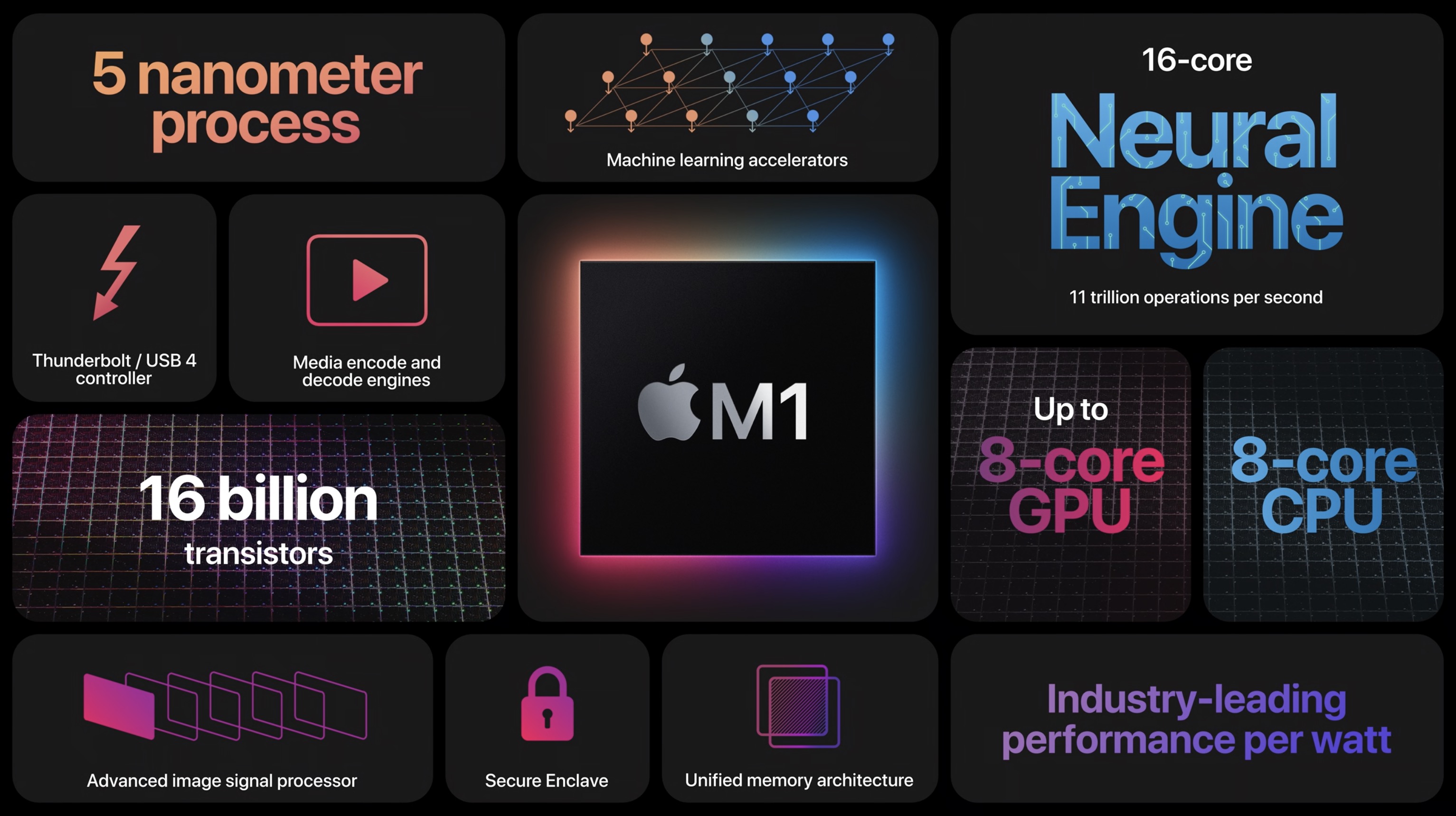
The Apple M1 is a System on a Chip (SoC) from Apple that is found in the late 2020 MacBook Air, MacBook Pro 13, and Mac Mini. It offers 8 cores divided in four performance cores and four power-efficiency cores. The big cores offer 192 KB instruction cache, 128 KB data cache, and 12 MB shared L2 cache. According to Apple the performance of these cores should be better than anything on the market (in late 2020). The four efficiency cores are a lot smaller and offer only 128 KB instruction cache, 64 KB data cache, and 4 MB shared cache. The efficiency cores (E cluster) clock with 600 - 2064 MHz, the performance cores (P cluster) with 600 - 3204 MHz.
The M1 is available in two TDP variants, a passive cooled 10 Watt variant for the MacBook Air and an active cooled faster variant for the MacBook Pro 13 and Mac Mini. Those should offer a better-sustained performance according to Apple.
The integrated graphics card in the M1 offers 8 cores (7 cores in the entry MacBook Air) and a peak performance of 2.6 teraflops. Apple claims that it is faster than any other iGPU at the time of announcement.
Furthermore, the SoC integrates a fast 16 core neural engine with a peak performance of 11 TOPS (for AI hardware acceleration), a secure enclave (e.g., for encryption), a unified memory architecture, Thunderbolt / USB 4 controller, an ISP, and media de- and encoders.
The Apple M1 includes 16 billion transistors (up from the 10 billion of the A12Z Bionic and therefore double the amount of a Tiger Lake-U chip like the i7-1185G7) and is manufactured in 5nm at TSMC.
Apple M2 Max
► remove from comparison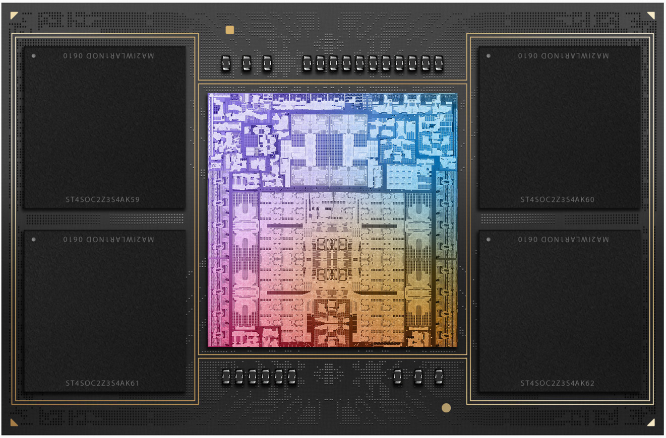
The Apple M2 Max is a System on a Chip (SoC) from Apple that is found in the early 2023 MacBook Pro 14 and 16-inch models. It offers all 12 CPU cores available in the chip divided in eight performance cores (P-cores) and four power-efficiency cores (E-cores). The E-cores clock with up to 3.4 GHz, the P-Cores up to 3.7 GHz (mostly 3.3 GHz in multi-threaded workloads and 3.4 GHz in single threaded).
The big cores (codename Avalanche) offer 192 KB instruction cache, 128 KB data cache, and 36 MB shared L2 cache (up from 24 MB in the M1 Pro). The four efficiency cores (codename Blizzard) are a lot smaller and offer only 128 KB instruction cache, 64 KB data cache, and 4 MB shared cache. CPU and GPU can both use the 49 MB SLC (System Level Cache).
The unified memory (32, 64, or 96 GB LPDDR5-6400) next to the chip is connected by a 512 Bit memory controller (400 GB/s bandwidth) and can be used by the GPU and CPU.
The CPU performance should be quite similar to the M2 Pro as only the higher memory bandwidth and bigger L3 cache could make a difference for some workloads.
The integrated graphics card in the M1 Max offers a 30-core GPU or a GPU with all 38 cores.
Furthermore, the SoC integrates a fast 16 core neural engine (faster than M1 Max), a secure enclave (e.g., for encryption), a unified memory architecture, Thunderbolt 4 controller, an ISP, and media de- and encoders (including ProRes).
The M2 Max is manufactured in 5 nm at TSMC (second generation) and integrates 40 billion transistors. The power consumption of the CPU part is up to 36 Watt according to powermetrics. When fully loading the CPU and GPU cores, the chip uses up to 89 Watt and the CPU part is limited to 25 Watt.
| Model | Samsung Exynos 2200 | Apple M1 | Apple M2 Max | ||||||||||||||||||||||||||||||||
| Codename | Exynos X2 / Cortex-A710 / A510 | ||||||||||||||||||||||||||||||||||
| Series | Samsung Exynos | Apple M1 | Apple M2 | ||||||||||||||||||||||||||||||||
| Clock | 1820 - 2800 MHz | 2064 - 3220 MHz | 2424 - 3696 MHz | ||||||||||||||||||||||||||||||||
| Cores / Threads | 8 / 8 | 8 / 8 | 12 / 12 | ||||||||||||||||||||||||||||||||
| Technology | 4 nm | 5 nm | 5 nm | ||||||||||||||||||||||||||||||||
| Features | 5G NR Sub-6GHz, 5G NR mmWave, LTE Cat. 24/22, LPDDR5-RAM, Dual-Core NPU, Wi-Fi 6E, Bluetooth 5.2 | ARMv8 Instruction Set | ARMv8 Instruction Set | ||||||||||||||||||||||||||||||||
| iGPU | Samsung Xclipse 920 ( - 555 MHz) | Apple M1 8-Core GPU | Apple M2 Max 38-Core GPU | ||||||||||||||||||||||||||||||||
| Architecture | ARM | ARM | ARM | ||||||||||||||||||||||||||||||||
| Announced | |||||||||||||||||||||||||||||||||||
| Manufacturer | semiconductor.samsung.com | ||||||||||||||||||||||||||||||||||
| Series: M2 |
|
| |||||||||||||||||||||||||||||||||
| L1 Cache | 2 MB | 3.3 MB | |||||||||||||||||||||||||||||||||
| L2 Cache | 16 MB | 36 MB | |||||||||||||||||||||||||||||||||
| L3 Cache | 8 MB | 48 MB | |||||||||||||||||||||||||||||||||
| Transistors | 16000 Million | 67000 Million | |||||||||||||||||||||||||||||||||
| Chip AI | 11 TOPS INT8 | 15.8 TOPS INT8 | |||||||||||||||||||||||||||||||||
| TDP | 79 Watt |

Benchmarks

Average Benchmarks Samsung Exynos 2200 → 100% n=9
Average Benchmarks Apple M1 → 182% n=9
Average Benchmarks Apple M2 Max → 258% n=9
* Smaller numbers mean a higher performance
1 This benchmark is not used for the average calculation