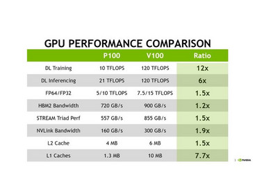
Nvidia first announced the Volta microarchitecture back in March 2013, presenting it as a successor to the Pascal microarchitecture that can be found in the GTX 1000 series today. Previous roadmaps showed that the first Volta GPUs could hit the market in Q3 2017, but Nvidia stated at the Hot Chips conference this year that Volta products are scheduled for an early 2018 release. Nvidia’s Tesla Chief Platform Architect, Rob Ober, was present at the conference and revealed some new details about the Volta GV100 chips.
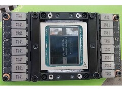
Using the TSMC 12 nm FinFET design and the SXM2 form factor, the GV100 has a massive die measuring 32 inch2, which is home for 21 billion transistors. Flanking the die are four stacks of HBM2 memory chips cumulating 16 GB. The GPU integrates 80 activated SMs - the equivalent of 5,120 CUDA cores. There are 4 additional non-activated SMs that offset any defects in the manufacturing process. The whole package where the die and memory chips reside draws an average of 300 W at 1 V.
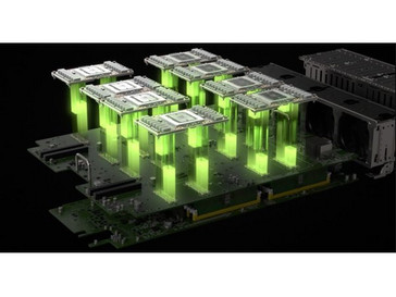
Nvidia also plans to release Tesla DGX-1 cards that pack eight Volta GPU chips into a 3U chassis. These cards are designed for professional use and are expected to deliver 960 TFLOPS from 40, 960 CUDA cores. Furthermore, the DXG-1 cards integrate 5,120 Tensor cores and six NVLink 2.0 connections that can develop a 3 TB/s throughput. A single DXG-1 card will draw up top 3.2 KW of power, so Nvidia had to come up with a new cooler design for these beasts.
The V100 chips will also be included in the upcoming gaming cards from the GeForce GTX series. The GTX 2080 is rumored to be priced at US$699 and is expected to hit the markets in early 2018, as well. It is supposed to bring greater efficiency and considerable performance gains for DX12 and Vulkan games.
I first stepped into the wondrous IT&C world when I was around seven years old. I was instantly fascinated by computerized graphics, whether they were from games or 3D applications like 3D Max. I'm also an avid reader of science fiction, an astrophysics aficionado, and a crypto geek. I started writing PC-related articles for Softpedia and a few blogs back in 2006. I joined the Notebookcheck team in the summer of 2017 and am currently a senior tech writer mostly covering processor, GPU, and laptop news.
> Expert Reviews and News on Laptops, Smartphones and Tech Innovations > News > News Archive > Newsarchive 2017 08 > Nvidia reveals more details on the upcoming Volta GPUs
Bogdan Solca, 2017-08-25 (Update: 2026-02-18)


