




Exclusive: 12.6 × 10.67 mm. That's the size of Qualcomm's next flagship chip, and we know more
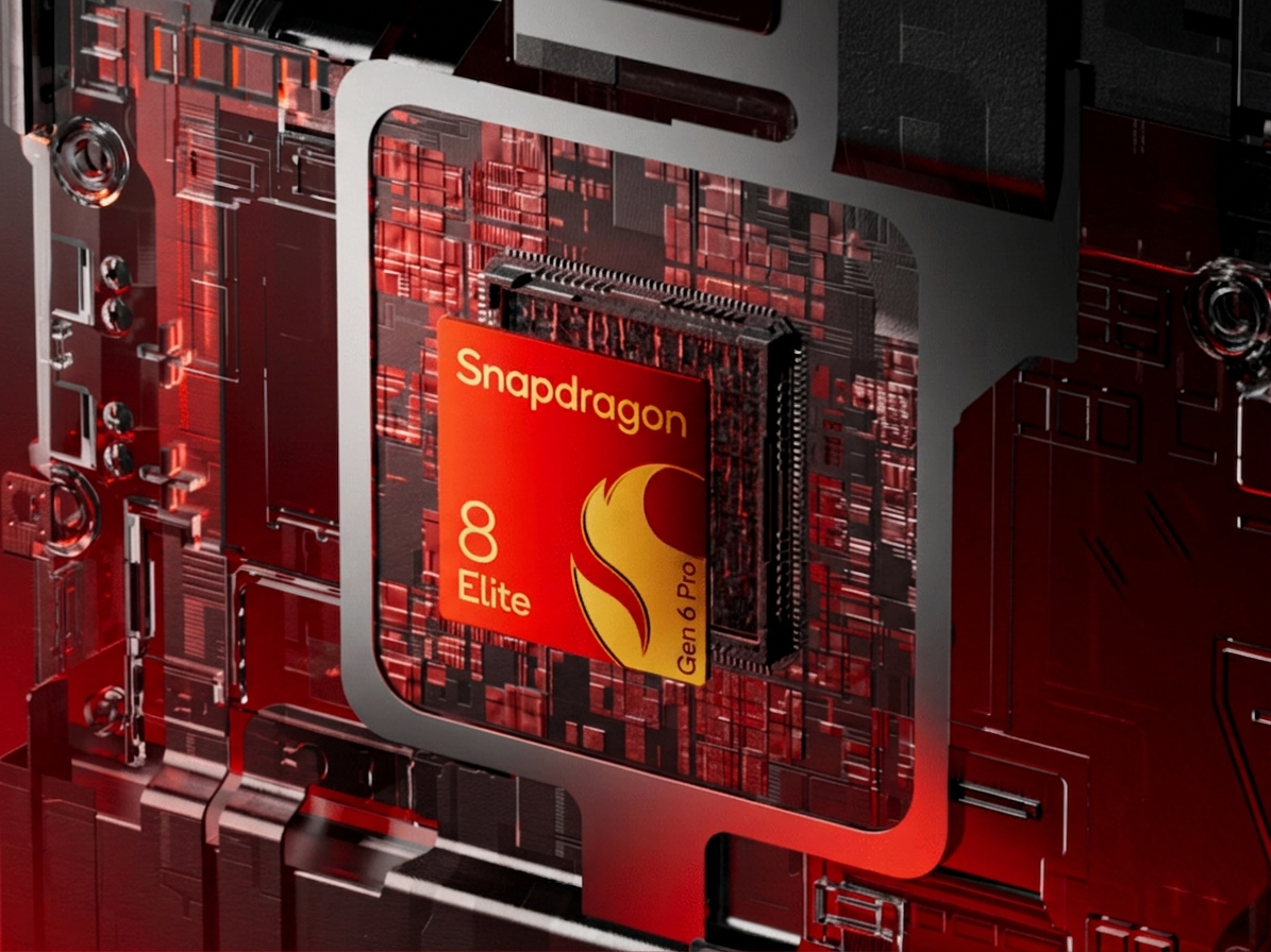
Qualcomm's next flagship platform, internally known as SM8975 and expected to launch as the Snapdragon 8 Elite Gen 6 Pro, is shaping up to be the company's biggest architectural jump in years. Based on a set of documents we've had a chance to review, a fairly complete picture of the chip has now emerged, from its die size and CPU layout down to its modem and RF specifications. Here's everything confirmed so far.
Die size
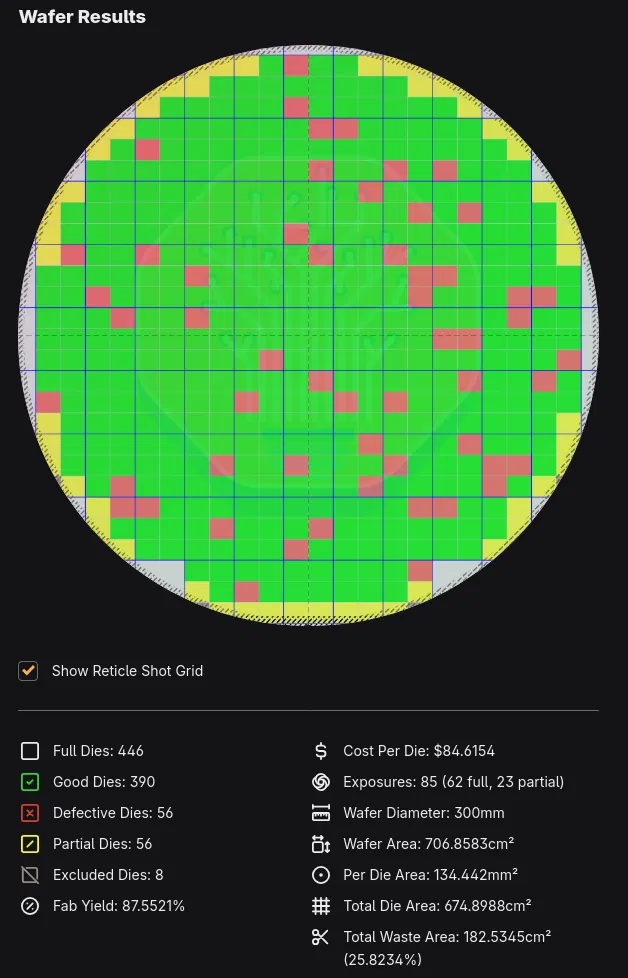
Our own measurement, calibrated against official package dimensions of 21.2 × 14 mm with a margin of roughly 1%, puts the SM8975 die at approximately 12.6 × 10.67 mm, or about 134 mm². That's larger than the Snapdragon 8 Elite Gen 5's confirmed 126.2 mm² die, despite the Gen 6 Pro's move to a smaller manufacturing process. The likely explanation is that the added complexity outweighs the density gains from the node shrink—more on that below. For context, that's still smaller than MediaTek's Dimensity 9500, which measures around 140 mm², suggesting that Qualcomm's jump to 2 nm is delivering real efficiency gains even with the added Matrix ALUs and cache on board.
Running that die size through a wafer-yield model, assuming a 300 mm wafer, a defect density of 0.1 defects/cm², and an estimated wafer cost of $33,000 for TSMC's N2P node, produces a raw silicon cost of roughly $84.62 per good die before packaging, testing, binning, or IP licensing costs are factored in. This is a modeled estimate built on assumed inputs; TSMC has not published N2P wafer pricing or defect-density figures, so it should be treated as a directional indicator of cost pressure rather than a confirmed BOM figure.
Process node
SM8975 reportedly moves to TSMC's N2P process, an enhanced 2 nm-class node and Qualcomm's first move beyond 3 nm for a flagship SoC. That puts it a full node ahead of the Snapdragon 8 Elite Gen 5's N3P process and slightly ahead of the Apple A20 Pro, which uses the baseline N2 process.
CPU
The chip carries a 2+3+3 Oryon core configuration: two prime cores, three performance cores, and three efficiency cores, continuing Qualcomm's custom Oryon architecture. Clock speeds have not been finalized in any documentation we've seen; claims circulating online of a peak clock speed of roughly 4.8 GHz remain unconfirmed and should be treated as speculative for now.
GPU
SM8975 pairs with the Adreno 850 GPU, up from the Adreno 840 in the outgoing SM8850. Graphics memory (GMEM) holds steady at 18 MB, matching the prior generation rather than increasing. The GPU driver stack adds a more granular DCVS (dynamic clock and voltage scaling) implementation that provides additional frequency steps, better jank detection and feedback mechanisms, and improved responsiveness across multiple simultaneous GPU contexts.
The supported API set remains consistent with that of the outgoing generation: OpenGL ES up to 3.2, OpenCL 3.0 FP, EGL 1.5, and Vulkan 1.4. This means that OEM driver-migration work should be minimal.
The standard SM8950 variant, by contrast, is expected to pair with a scaled-down Adreno 845 and 12 MB of GMEM, underlining the gap Qualcomm appears to be creating between its standard and Pro flagship tiers this generation.
Matrix ALUs and AI Frame Fusion
New to this generation are two dedicated Matrix ALU blocks within the GPU's shader processor. Purpose-built to accelerate GEMM and convolution operations, which form the mathematical foundation of most on-device AI workloads, they underpin a new feature called AI Frame Fusion, Qualcomm's take on AI-driven upscaling and frame interpolation. Both the Matrix ALU blocks and AI Frame Fusion appear to be specific to the Adreno 850 in the SM8975. The Adreno 845 in the standard SM8950 reportedly lacks them, making this another Pro-exclusive differentiator alongside the larger GMEM allocation.
AI Frame Fusion operates in two modes. A super-resolution mode combines motion vectors, a depth buffer, a low-resolution color buffer, and the previously rendered frame to upscale the output to 1080p or 1440p. A separate frame-generation mode uses motion-vector and optical-flow reprojection across the current and previous frames to interpolate an entirely new frame between them, with the aim of boosting perceived frame rates without a proportional rise in power draw. Both modes use the new Matrix ALUs together with the GPU's GMEM pool to improve on-chip efficiency.
Cache and memory
SM8975 is reported to carry a shared 16 MB L2 cache alongside an 8 MB system-level cache, a jump from the current generation's configuration. As for memory, the Pro variant supports both LPDDR5X and the incoming LPDDR6 standard, while the standard SM8950 support only LPDDR5X, a segmentation choice likely driven by LPDDR6 pricing amid the ongoing DRAM supply crunch.
Modem
The Pro variant is paired with Qualcomm's new X105 modem, which has not previously appeared on a shipping Snapdragon platform. Both SM8975 and the standard SM8950 (Snapdragon 8 Elite Gen 6) are reported to share the same RF front end, which is said not to be backward-compatible with older modems. The base variant is therefore likely to ship with the X105 as well, possibly in a cut-down configuration, rather than reuse a prior-generation modem.
Connectivity
Two companion chips have surfaced for wireless connectivity: the WCN8841 and WCN8851, both of which belong to the FastConnect 8800 lineup. Both support Wi-Fi 8 in a 2×2, 300 MHz MIMO configuration, along with Bluetooth HDT on the 2.4 GHz band and support for Thread. They differ by tier: the 8841 supports Bluetooth 6.0, while the 8851 steps up to Bluetooth 7.0 and adds a second Wi-Fi radio path capable of 2×4/4×4 MIMO at 320 MHz, Bluetooth 7.0 support on the 5 GHz and 6 GHz bands, and ultra-wideband (UWB).
On the modem-RF side, two transceivers are associated with this generation. The SDR765 is a sub-6 GHz-only part built on TSMC's N6RF node, marking a shift away from Samsung's previously used 14 nm RF process and matching the RF node used in the Apple C1 modem-RF system. It supports 2×2 MIMO uplink and 4×4 MIMO downlink, with 1024-QAM modulation and support for the n253, n255, and n256 satellite bands.
The SDR885 is the more significant of the two: it is Qualcomm's first sub-6 GHz transceiver to support 4×4 MIMO on both uplink and downlink simultaneously, meaning that upload throughput can now match download throughput for the first time on a Snapdragon platform. It supports 256-QAM uplink and 1024-QAM downlink, as well as both sub-6 GHz and mmWave under the 3GPP Release 18 framework, with 20 transmit ports (arranged 7+7+3+3) and 16 primary plus 16 diversity receive-input paths.
Positioning, cost, and expected devices
Qualcomm's pricing strategy this generation appears to split the flagship tier more sharply than before. The SM8975 is expected to carry meaningfully higher production costs than the standard SM8950, a gap likely to be widened further by LPDDR6 pricing, and may be reserved for a smaller set of ultra-premium devices rather than the full flagship lineup. It is worth noting that the "significantly higher production cost" figures circulating from tipster sources typically describe the full platform price OEMs pay, including the RF transceivers and FastConnect wireless chip bundled with the SoC itself, rather than the raw die cost in isolation. That's a meaningfully different figure from the roughly $84.62-per-die silicon estimate above, and the two shouldn't be conflated.
Launch timing
SM8975 is expected to launch at Qualcomm's Snapdragon Summit, which is officially confirmed to run in Maui, Hawaii, from September 22 through September 24, 2026. Xiaomi is widely expected to be first out of the gate with a Snapdragon 8 Elite Gen 6-powered device, potentially unveiling the Xiaomi 18 series in China alongside Qualcomm's keynote. Commercial devices from other OEMs are expected to follow later in the year and into early 2027.
Source(s)
 Add as a preferred source on Google


