Apple A19 Pro die shot showcases smaller profile chip with minimal design changes
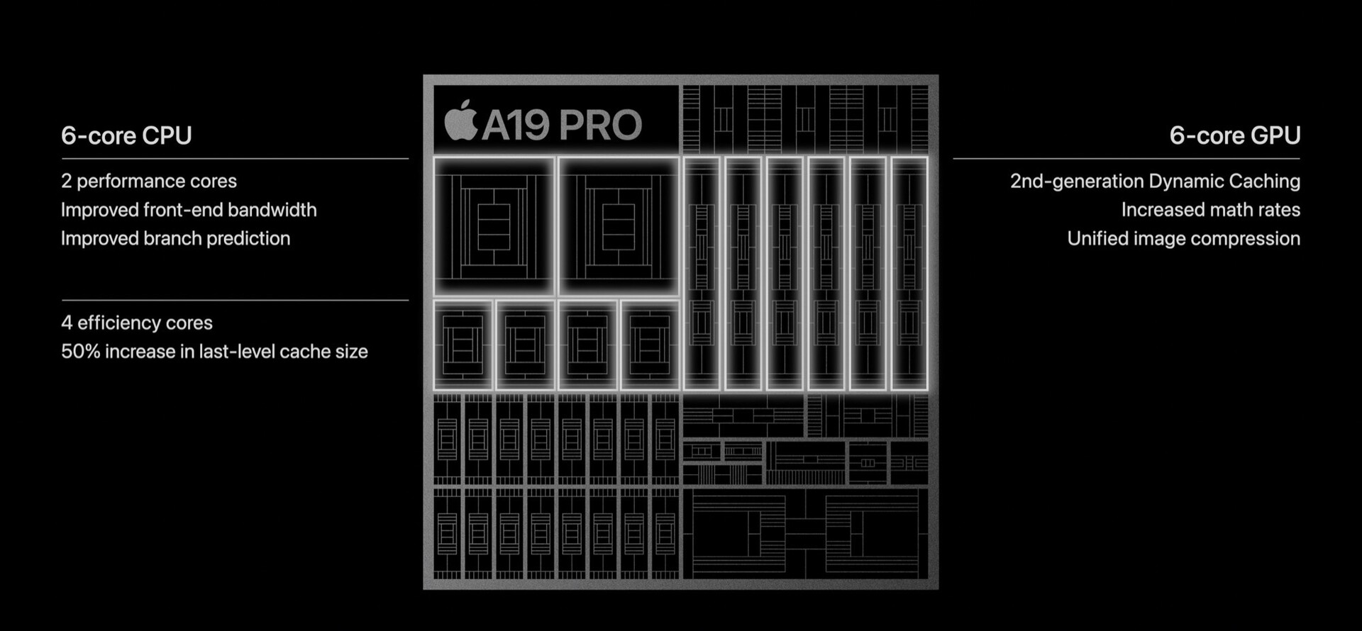
After posting detailed teardowns of the Snapdragon 8 Elite Gen 5 and Dimensity 9500, X semiconductor expert @KurnalSalts has now posted an in-depth die shot of Apple's latest flagship SoC, the A19 Pro. MediaTek had to ramp up die area to meet performance requirements. Qualcomm managed to keep more or less the same die size.
Apple, on the other hand, actually reduced its die area from 105 mm2 to 98.6 mm2. That is mainly possible due to its use of TSMC's cutting-edge N3P node, which allows Apple to pack more transistors in the same area. The A19 Pro variant in question here is the full-fat one with six GPU cores. Not much has changed design-wise, with the A19 Pro essentially using the same structure as the A18 Pro (TSMC N3E) and the A17 Pro (TSMC N3B) before it.
We might see some differences in the next-gen A20/A20 Pro because it is expected to use TSMC's N2 node- the first of its kind to use a gate-all-around design, allowing for even more transistor density and thus a noticeable increase in performance.
