3D chips: Smartphones might make a big leap in performance as MIT researchers unveil new tech
For years, the electronics industry has sought to use gallium nitride (GaN) in complex circuits. GaN is a semiconductor that is faster and more power-efficient than silicon, but its high cost has limited its use. Conventional methods that bond entire GaN wafers to silicon are expensive, hindering widespread adoption.
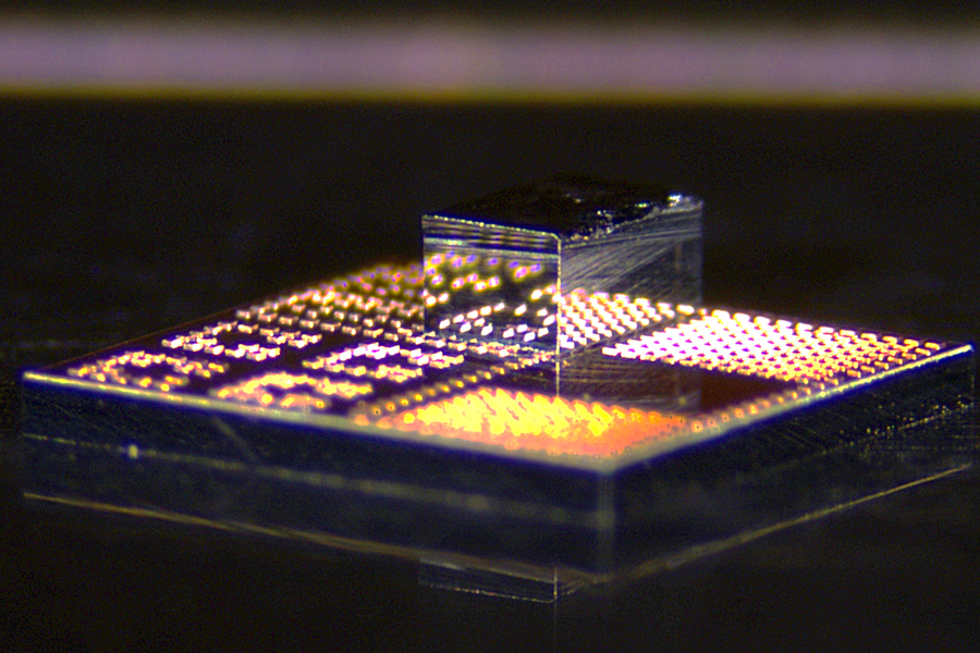
The new process eliminated the use of a GaN wafer alongside silicon and opted for GaN transistors on silicon wafers. As a result, the new process cut costs and boosted speed and efficiency. This process was invented by MIT researchers alongside industry partners.
The researchers did this by cutting out individual GaN transistors, called 'dielets', which measure 240 by 410 microns. Each transistor is made with tiny copper pillars on top, which they use to bond directly to the copper pillars on the surface of a standard silicon CMOS chip. This use of low-temperature copper-to-copper bonding technique is cheaper, more conductive, and more compatible with standard semiconductor foundries than traditional methods that use gold for bonding.
The team used this process to fabricate a power amplifier that achieved higher signal strength than the silicon-only chips currently used in smartphones while using less power. This shows prospect for use in 5G/6G and IoT devices. The chips also show promise for quantum computing, as GaN thrives at low temperatures.
If this technology is commercialized, smartphones and other consumer devices could see a significant boost in performance, providing the power needed for more advanced on-device AI models. In the meantime, the Samsung Galaxy S25 Ultra (curr. $1,219 on Amazon) remains one of the most powerful smartphones with on-device AI capabilities.
NB: No detailed performance statistics/comparisons were reported.
Source(s)
