TSMC’s second Kumamoto fab reportedly slips to 2029 as attention shifts to U.S. expansion
TSMC’s plan to expand its footprint in Japan has encountered delays, with its second Kumamoto plant now expected to begin volume production only in the first half of 2029—roughly eighteen months later than the most recent roadmap suggested, according to Nikkan Kogyo Shimbun via MoneyDJ.
The timeline for construction has also shifted. The project was originally pencilled in for a ground-breaking in the first quarter of 2025, then quietly pushed to “sometime in 2025.” TSMC chair and CEO C.C. Wei attributed the slip to congestion and other traffic issues around the site; subsequent reporting by The Wall Street Journal adds that the company is diverting resources to its U.S. fabs to navigate tariff policy, making the new start date hard to pin down.
Market dynamics appear to be another headwind. Economic Daily News notes that the 6 nm and 7 nm processes planned for Kumamoto 2 target clients such as Sony and Denso. However, current Japanese demand for such advanced nodes remains limited, which reduces the incentive for rapid build-out and contributes to the project delay.
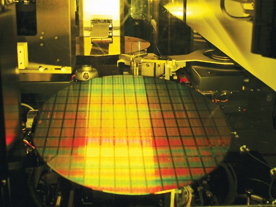
Despite challenges with Kumamoto 2, Kumamoto 1 has moved smoothly into mass production. Wei told investors that the first plant, focused on 12 nm to 28 nm chips, entered volume production in the second half of 2024 and is already achieving good yields.
Looking ahead, the two facilities are still expected to deliver more than 100,000 12-inch wafer equivalents per month once both are operational. The total investment remains around ¥2.96 trillion (~$20.04 billion), with up to ¥1.2 trillion (~$8.12 billion) in subsidies provided by the Japanese government. Whether that capacity arrives on schedule now depends on how quickly infrastructure bottlenecks are cleared—and on how demand for advanced Japanese automotive and imaging chips evolves over the remainder of the decade.
Source(s)
TrendForce (in English)
