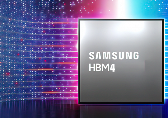
Samsung and SK Hynix rumored to boost AI accelerator performance with the advent of the HBM4 DRAM standard
HBM DRAM is still expensive compared to the GDDR solution we see integrated with consumer video cards, but the price mostly justifies the performance gains. This is why HBM is supplied with HPC and AI accelerators for the time being. It is also the reason why the Nvidia’s latest H100 cards cost so much as they pack HMB3E DRAM. South Korean sources close to DigiTimes claim that the situation could soon change with the introduction of the HBM4 standard that doubles the memory bus width over the previous version.
According to DigiTimes, HBM4 will be the most important upgrade in the history of HBM DRAM since it will increase the stack bus width from 1024-bit to 2048-bit. The current HBM3 standard boasts ~9 GT/s per chip leading to a 1.15 TB/s peak bandwidth for all stacks. If the HBM4 standard will maintain the same number of stacks, peak bandwidth could essentially reach 2.30 TB/s.
Take the Nvidia H100, for example. This card features six 1024-bit HBM3E known good stack dies (KGSDs) combining for a 6144-bit interface. Due to concerns regarding increased difficulty to manufacture memory stacks with more than 1,024 through silicon vias, Samsung and SK Hynix will need to prove they can indeed keep the same number of stacks while increasing the bus width to 2048-bit, despite claims of near-100% yields.
Buy the Nvida H100 compute card with 80 GB HBM2E RAM on Amazon
Source(s)
