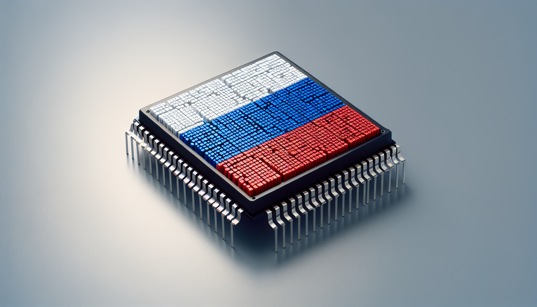
Russia is developing a 11.2 nm EUV lithography system to rival ASML's technology
Russia is gearing up to build its own extreme ultraviolet (EUV) lithography machines. Still, it's taking a different route with an 11.2 nm wavelength technology instead of the more common 13.5 nm used by ASML's systems. Nikolay Chkhalo from the Russian Academy of Sciences' Institute of Microstructure Physics is leading the charge, hoping to make lithography gear that's cheaper and less complicated.
These new Russian EUV machines will use lasers powered by xenon, steering away from ASML's tin-based approach. Chkhalo claims that this 11.2 nm wavelength brings a 20 percent bump in resolution and could make designing the optics easier while keeping manufacturing costs down. Plus, they aim to reduce contamination in the optical elements, which should help key parts-like collectors and protective pellicles-last longer.
Here's the plan laid out in three steps:
- Start with research: Nail the essential tech and test out components.
- Build a prototype: A machine that can handle 60 200-mm wafers per hour.
- Go big: A production-ready system working on 60 300-mm wafers per hour.
That said, these machines won't be as fast as ASML's. They'll run at about 37 percent of ASML's throughput, using a 3.6 kW light source. While that's not great for high-volume production, it's good enough for smaller-scale manufacturing.
Switching to the 11.2 nm wavelength means they need to create a whole new ecosystem-like special mirrors, coatings, mask designs, and photoresists. Even the chip design software tools need some heavy reworking, especially for mask data prep and optical corrections.
They haven't nailed down a timeline for these development steps yet, but experts think building a complete lithography ecosystem could take ten years or more. They also haven't revealed which process nodes these new tools will support.
Source(s)
CNews (in Russian)
