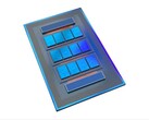
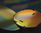
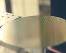
Intel recently managed to integrate two state-of-the-art ASML High-NA EUV lithography machines into its production line, with a reported higher reliability compared to previous models. Steve Carson, one of Intel’s top engineers, shared that the company processed 30,000 wafers in just a single quarter with these advanced systems.
Last year, Intel became the first in the industry to receive the High-NA Twinscan EXE:5000 EUV lithography tools, setting them up at its D1 development facility near Hillsboro, Oregon. Although ASML sees these machines as pre-production tools—not quite built for high-volume manufacturing—Intel’s early results are pretty encouraging.
This quick adoption marks a notable strategic shift for Intel. In the past, they were lagging behind competitors when it came to rolling out the earlier generation of extreme ultraviolet lithography machines, taking a full seven years to integrate them into production. That delay was one of the factors that saw Intel lose its manufacturing edge to TSMC.
The new High-NA machines bring some significant technical advantages. They can achieve resolutions down to 8nm in a single exposure, an improvement from the 13.5nm resolution of the older Low-NA systems. This means that tasks which used to need three exposures and around 40 processing steps can now be done with just one exposure and only a handful of steps.
Currently, Intel is putting these High-NA tools to the test with its 18A manufacturing technology, with plans to move them into full production alongside its upcoming 14A (or 1.4nm-class) tech. They’ve already scheduled mass production of a new generation of PC chips using the 18A technology later in 2025, though the rollout for 14A is still under wraps.
Source(s)
Reuters (in English)


