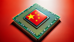
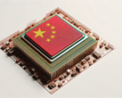
JFS Laboratory, a government-supported company, has just rolled out the country's very first silicon photonics chip. This is a pretty exciting step forward for things like AI and high-performance computing, which need that extra boost.
Silicon photonics uses lasers for input and output instead of the usual copper wires, which has some incredible perks. We're talking about way more bandwidth, less waiting around (latency), and better energy savings—all significant for ramping up AI and HPC systems to match the growing demands.
According to the South China Morning Post, JFS Laboratory was set up in 2021 with a hefty government backing of 8.2 billion yuan (that's about $1.2 billion). After three years of hard work, they've managed to stick a laser light source onto a silicon chip. But, they're keeping things under wraps when it comes to specifics like how fast the data transfer is or how much power it sucks up.
This breakthrough is a big deal for China's chip-making dreams. With optical interconnects, they can create chip designs that can handle the heavy computational load AI and HPC need while being energy-conscious, which is important for massive data centers.
Plus, this tech could help bring down the costs for data centers since optical signals don't heat things as much and use less power over long distances compared to traditional copper.
While we still need to get all the nitty-gritty details on JFS Laboratory's silicon photonics chip, pulling off this tech marks a notable advancement for China's semiconductor aspirations.
Source(s)
SCMP (in English)


